 language
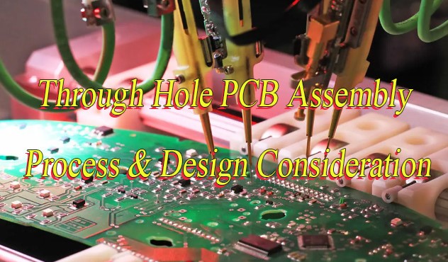
Through Hole PCB Assembly Process & Design Consideration
Through hole PCB assembly remains a trusted manufacturing approach, even as electronics continue to move toward smaller and lighter designs. While surface mount technology dominates many consumer products, through-hole methods still play a critical role in applications that demand strength, durability, and long service life. This is especially true in industrial control, power electronics, automotive modules, and equipment exposed to vibration or thermal stress.
This article will explain how the through-hole PCB assembly process works, important design rules, quality control methods, and how to choose a reliable through-hole PCB assembly manufacturer.
What is Through Hole PCB Assembly?
Through hole PCB assembly is a method where component leads pass through plated holes in the circuit board and are soldered on the opposite side. This creates a strong mechanical bond between the component and the PCB.
Unlike surface mount parts that sit on pads, through-hole components anchor themselves within the board structure. As a result, they tolerate vibration, shock, and mechanical stress more effectively. This is why many designers still rely on through-hole PCB assembly services for demanding environments.
In practice, this method supports components such as connectors, transformers, large capacitors, and power devices. These parts benefit from the added strength that through-hole mounting provides.
Why Choose Through Hole PCB Assembly Services?
Advantages of Through Hole PCB Assembly Services:
- mechanical strength stands out. The solder joint wraps around the lead and the plated hole. This structure resists pull-out forces far better than surface-mounted joints.
- thermal tolerance matters. Through-hole components often handle higher power levels. They dissipate heat more effectively, especially when paired with thicker copper layers.
- reliability over time remains a strong advantage. In harsh environments, solder joints face temperature cycles and vibration. Through-hole connections tend to degrade more slowly.
- repair and modification are easier. Individual components can be replaced without specialized rework equipment. This matters for long-life products and field service.
Difference Between Through-Hole PCB Assembly vs SMT
| Comparison Aspect | Through-Hole PCB Assembly | SMT (Surface Mount Technology) |
| Component Installation | Leads pass through drilled holes, soldered opposite side | Mounted directly on surface pads |
| Mechanical Strength | Strong bonding, excellent vibration/shock resistance | Smaller solder joints, lower mechanical strength |
| Suitability | High-power/high-current components (e.g., connectors, transformers) | Compact/lightweight designs, high component density |
| Assembly Speed & Labor | Slower (often manual insertion), higher labor cost in low-mid volumes | Faster (automated pick-and-place), lower cost at high volumes |
| Repair/Maintenance | Easier to repair/replace components | More difficult, requires specialized equipment |
| Space Efficiency | Requires more board space (due to hole drilling) | Space-efficient, supports miniaturization |
| Stress Resistance | Ideal for mechanically stressed components | Less suitable for heavy/mechanically stressed components |
| Production Priorities | Prioritizes strength, durability, and reliability | Prioritizes size reduction, production efficiency, and cost at scale |
| Typical Applications | Industrial controls, power electronics, large capacitors | Consumer electronics, high-density circuits, mass production |
| Combined Use | Often combined with SMT on modern boards for optimal results | Complementary to through-hole in hybrid designs |
Through Hole PCB Assembly Design Consideration
Here are Design Consideration for Through Hole PCB Assembly:
- Optimal Hole Sizing Based on Component Leads: IPC-7251 defines three density levels for through-hole components: maximum (A), nominal (B), and minimum (C). Hole diameter should equal lead diameter plus 0.25mm (A), 0.20mm (B), or 0.15mm (C) to ensure proper solder infiltration and mechanical stability. This margin prevents lead damage and plating delamination during assembly.
- Annular Ring Requirements for Reliability: IPC-2221 specifies minimum annular ring sizes to maintain solder joint integrity. A ring width of at least 0.1mm ensures adequate solder coverage and mechanical strength. Insufficient rings risk pad lifting during thermal cycling, compromising long-term reliability.
- Thermal Management Through Pad Design: High-power components require larger pads or thermal vias to dissipate heat. Increasing pad size by 30-50% reduces thermal resistance, while adjacent thermal vias (0.3-0.5mm diameter) enhance heat transfer to ground planes, preventing solder joint failure.
- Signal Integrity via Minimal Parasitic Paths: Place through-holes close to power/ground pins to reduce lead length, minimizing inductance. Short leads (<2mm) and thick power traces (≥0.5mm) lower impedance, improving signal integrity in high-speed designs.
- Spacing Constraints for Manufacturability: Maintain a minimum spacing of 0.25mm between through-hole pads to prevent solder bridges. For dense layouts, use a spacing of D1 = D2 + 0.41mm (where D1 is hole-to-hole distance, D2 is pad-to-pad distance) to accommodate manufacturing tolerances.
- Layer-Specific Via Placement for Density: In multi-layer boards, align through-holes vertically across layers to minimize signal path length. Use blind/buried vias for critical traces to reduce parasitic capacitance and improve routing efficiency without compromising signal quality.
- Wave Soldering Compatibility: Design pads with a 2-3mm solder mask-defined edge to prevent solder wicking during wave soldering. Flux application prior to soldering ensures proper wetting, while a 1-2mm solder fillet height confirms acceptable joint formation per IPC-A-610G.
- Component Placement for Assembly Efficiency: Group related components to minimize jumper wires and solder joints. Position heavy components (e.g., transformers) near board edges to reduce mechanical stress during handling, while placing test points near ports to facilitate debugging and testing.
- Material Selection for Environmental Stress: Choose FR-4 or high-Tg substrates (Tg ≥ 170°C) for thermal stability. Thicker copper traces (≥1oz) reduce resistance in power paths, while solder mask thickness (≥0.02mm) protects pads from mechanical damage during assembly.
- Cost-Performance Balance: Prioritize through-hole for high-reliability applications (e.g., aerospace) where mechanical robustness outweighs density needs. For high-density designs, combine through-hole with SMT components using selective soldering to optimize cost and performance.
What is the Through-Hole Assembly Process of PCB?
Below is Through Hole PCB Assembly Process:
1. PCB and Component Verification
- Validate PCB surface integrity per IPC-A-610: ensure no visible damage, hole misalignment ≤0.05mm, and silkscreen contrast ≥0.8 for readability.
- Verify component specifications via BOM traceability; inspect leads for oxidation/bending using AOI systems, reducing defect rates by 15%.
- Bake moisture-sensitive components at 125°C for 8–12 hours (per J-STD-033) to prevent solder joint cracking, extending shelf life by 50%.
2. PCB Surface Preparation
- Clean surfaces via ultrasonic bath with DI water and mild detergent, achieving <1mg/cm² residual contamination.
- Apply OSP or HASL coatings per IPC-SM-840C to boost solderability by 30%; maintain coating thickness of 0.1–0.3μm for optimal results.
- Use adhesive dots for mechanical stabilization of components >10g, reducing vibration-induced failures by 20%.
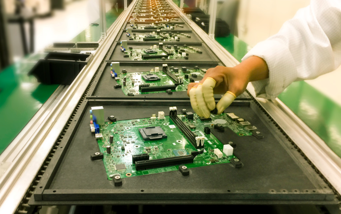
3. Component Placement Techniques
- Manual insertion for prototypes/repairs: achieve 99.5% accuracy with magnification tools; suitable for irregular shapes and low-volume runs.
- Automated insertion for high-volume: operate at 10,000–15,000 components/hour with 99.9% accuracy, reducing labor costs by 40%.
4. Soldering Process Parameters
- Wave soldering: preheat PCB to 90–110°C, solder at 240–260°C, and cool at 3–5°C/s. This minimizes thermal shock and solder voids by 25%.
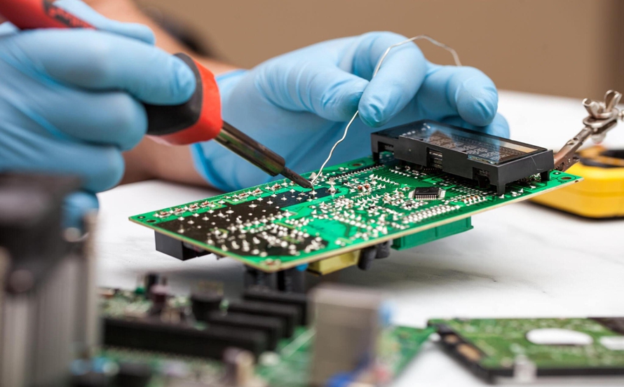
- Hand soldering for selective repairs: use 350–400°C irons with 1–3s contact time per joint, ensuring 98% joint integrity and reducing rework by 30%.
- Dip soldering (legacy designs): maintain solder pot at 230–250°C with 2–4s immersion, achieving 95% wetting and 20% faster setup than wave methods.
5. Post-Assembly Processing
- Trim component leads to 1–2mm above PCB using automated cutters, reducing short-circuit risks by 40% and improving electrical clearance.
- Clean assemblies with water-soluble fluxes via deionized water rinses, achieving <0.5μg/cm² ionic contamination for high-reliability applications.
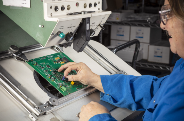
6. Quality Inspection and Testing
- Manual visual inspection: check for 100% solder joint coverage, correct polarity, and no visible defects; achieve 99% defect detection with trained operators.
- AOI systems scan at 0.1mm resolution, detecting 98% of defects (e.g., bridging, insufficient solder) with 2ms per inspection point.
- ICT provides 99% circuit verification coverage via bed-of-nails testing; FCT validates functional performance with 95% test coverage for end-product reliability.
- X-ray AXI detects hidden solder joints (e.g., BGAs) with 5μm resolution, ensuring 99% defect detection in high-density assemblies.
Quality Control & Reliability Testing for Through Hole PCB Assembly
Process Quality Control Across Assembly
- Component incoming inspection: verify lead dimensions per IPC-J-STD-001, confirm no oxidation/deformation via 20x magnification, and validate electrical performance with LCR meters (≤1% tolerance).
- Insertion accuracy management: ensure lead-to-hole clearance of 0.1–0.2mm using automated insertion machines, reducing misplacement errors by 35% compared to manual methods.
- Soldering parameter monitoring: maintain wave soldering conveyor speed at 0.8–1.2m/min, preheat temperature at 90–110°C, and solder pot temperature at 250±5°C to minimize voids (<5% void area per IPC-A-610).
Solder Joint Quality Inspection
- Visual inspection with 50x magnification: check for 100% solder coverage, void-free joints (void diameter ≤0.1mm), and fillet formation meeting IPC-610 Class 2/3 standards.
- X-ray inspection for critical assemblies: achieve 5μm resolution to detect internal voids in through-hole joints, ensuring ≥75% solder fill for reliability in thermal cycling (-40°C to 125°C).
Mechanical Reliability Verification
- Lead pull test: apply 5–15N force per lead (per IPC-610) to confirm solder joint integrity, with failure rates ≤0.1% after 500 thermal cycles.
- Vibration testing: subject assemblies to 3-axis random vibration (5–500Hz, 5G RMS) for 2 hours, ensuring no component displacement or solder cracking.
- Drop testing: perform 26-drop sequence (1m height) per IEC 60068-2-31, verifying no electrical failures or structural damage.
Electrical & Environmental Reliability Testing
- Electrical tests: conduct insulation resistance (≥100MΩ at 500VDC), continuity (<1Ω per trace), and dielectric withstand (1000VAC for 1 second) per IPC-9261.
- Environmental tests: cycle between -55°C and 125°C for 100 cycles (30-minute dwell per condition), and 96-hour 85°C/85% RH testing to validate long-term stability.
Defect Management & Traceability
- Non-conforming product handling: classify defects (e.g., cold solder, misaligned leads) using ISO 13485-compliant systems, with corrective actions reducing defect recurrence by 40%.
- Batch traceability: implement QR-code tracking for each PCB lot, storing inspection data in SQL databases for 10-year retention, enabling full process traceability and trend analysis.
How Much Does Through Hole PCB Assembly Cost?
Through-hole PCB assembly costs depend on key production factors. Labor is the main cost driver due to manual/semi-automatic insertion for boards with many leads or complex components, increasing handling time. Component type impacts costs too, large, heavy, or custom-shaped parts need slower, precise insertion and soldering. Board complexity, like dense layouts or mixed SMT/THT technologies, slows insertion and requires more inspection. Production volume inversely affects costs: low volumes use manual processes with higher per-unit costs, while high volumes leverage wave solder optimization and efficiency.
How to Choose A Reliable Through Hole PCB Assembly Manufacturer?
A Selection Guide to Through Hole PCB Assembly Manufacturer:
- Certification Audit: Prioritize vendors with ISO9001, ISO14001, and industry-specific certifications (e.g., IATF16949 for automotive). Confirm strict adherence to IPC standards like IPC-A-610 and J-STD-001 for assembly quality compliance.
- Process & Equipment Evaluation: Assess dual wave soldering, X-ray inspection, and precision insertion equipment. Verify board thickness/hole ratio capability (≥10:1 standard, ≥12:1 advanced), soldering parameter control (110-130°C preheat, 3-5s soldering), and support for hybrid/SMT/thick-copper assembly.
- Quality Control System: Ensure end-to-end coverage via MES traceability, strict incoming material checks (pin specs, appearance, electrical performance), real-time process monitoring (temperature, flux usage), and comprehensive final testing (continuity, insulation, pull tests). Target FTR >95% with closed-loop defect optimization.
- Supply Chain & Delivery: Require BOM sourcing support with ≥80% authorized distributor components. Confirm delivery timelines: ≤5-day pilot production, scalable mass production, and material shortage contingency plans.
- Case Studies & Customization: Select vendors with relevant project experience (e.g., high-power/vibration assembly). Request past project parameters, quality reports, and client feedback. Verify customization support (e.g., special hole sizes) with design-side technical assistance.
- After-Sales Service: Define technical support response times, defect return processes, liability allocation, and warranty periods. Ensure dedicated engineering teams for design-process compatibility troubleshooting and optimization.
FAQs of PCB Through Hole Assembly
Q1: What types of components are best suited for PCB through hole assembly?
A1: PCB through hole assembly is ideal for components that are large, heavy, or subject to mechanical stress. Common examples include connectors, transformers, power inductors, electrolytic capacitors, and high-current devices.
Q2: Is wave soldering always required for PCB through hole assembly?
A2: No. While wave soldering is widely used for volume production, PCB through hole assembly can also be completed using selective soldering or manual soldering, depending on board design and production volume.
Q3: How does hole size affect PCB through hole assembly quality?
A3: Proper hole size ensures smooth component insertion and strong solder joints. Holes that are too small can damage plating, while oversized holes may lead to weak solder connections and inconsistent fill.
Q4: What inspections are commonly used in PCB through hole assembly?
A4: Visual inspection is standard for checking solder fillets and lead protrusion. AOI may be used for consistency checks, and electrical testing verifies continuity and isolation. High-reliability products may include additional testing.
Q5: Does PCB through hole assembly impact product lifespan?
A5: Yes. The strong mechanical bonding created by PCB through hole assembly helps components withstand vibration, thermal cycling, and long-term use, which can significantly extend product lifespan in demanding environments.