 language
Reliable Blind Via Hole Solutions for High-Density PCB Design
Blind Via Hole is a critical interconnect technology that connects an outer layer of a printed circuit board to one or more inner layers without penetrating the entire board. This article provides a comprehensive guide to understanding blind vias, their benefits, trade-offs, and optimal applications in modern electronics.
Are you struggling to balance these competing demands?
- Severe routing congestion on dense multilayer boards, especially around fine-pitch BGAs
- Unpredictable HDI costs that quickly push projects over budget
- Signal integrity issues caused by long via stubs in high-speed designs
- Limited supplier capability for stacked or high-aspect-ratio microvias
- Wasted routing space from traditional through-holes that don’t connect every layer
These challenges demand a partner with robust technical expertise. The solution lies in collaborating with a manufacturer that masters advanced HDI processes.
- Expert DFM Support: Blind via and microvia layouts optimized early for yield and reliability
- Transparent Cost Engineering: Clear insight into blind via cost drivers before fabrication begins
- Stack-Up & Material Guidance: Proven laminate and prepreg selection for blind via hole PCB reliability
- Precision Drilling & Plating: Consistent blind vias in PCB through controlled laser drilling and plating
- Mature HDI Process Control: Stable blind via process for blind via buried via structures
At EBest Circuit (Best Technology), we are a professional PCB manufacturer specializing in high-density interconnect (HDI) technology. Our expertise lies in delivering reliable, high-performance boards featuring complex blind vias and buried vias in PCB. We combine state-of-the-art equipment with deep engineering experience to turn your most challenging designs into manufacturable reality. Pls feel free to contact our team at sales@bestpcb.vn to discuss your project.
Blind Via Hole Definition: What a Blind Via Hole Really Means in Modern PCB Design
In essence, a blind via hole is a plated through-hole that starts on an outer layer of a PCB and terminates at an internal layer, without going through the entire board thickness. It is a foundational element of HDI design, enabling more efficient use of space.
- Primary Function: To create an electrical connection between a surface layer and a subsurface layer.
- Key Characteristic: The hole has a defined, non-through depth.
- Formation: Typically created using precision laser drilling after the relevant core layers are laminated.
- Visual Identification: On a finished board, a blind via is visible only on one side (the side it starts from).
The blind via hole definition centers on its role as a space-saving interconnect. Unlike a standard through-hole via, it does not create a “through” hole, thereby preserving routing channels on layers it does not need to connect. This makes it indispensable for compact, high-pin-count components like modern processors and FPGAs.
How Blind Vias in PCB Improve Routing Density and Signal Integrity
Implementing blind vias in PCB delivers two paramount advantages: dramatic space savings and enhanced electrical performance. This section breaks down how they achieve this.
- Increased Routing Channels: By eliminating through-holes on unrelated layers, blind vias free up valuable real estate for additional signal traces.
- Escape Routing for BGAs: They allow direct connections from inner BGA ball pads to the required internal signal layers, simplifying fanout.
- Reduced Via Stub Length: In high-speed design, the unused portion of a via (the stub) acts as an antenna. Blind vias inherently have shorter or non-existent stubs, minimizing signal reflection and attenuation.
- Improved Power Delivery Network (PDN): Shorter, more direct paths from power planes to device pins reduce inductance and improve transient response.
- Layer Count Optimization: Often allows for the same functionality with fewer total layers compared to using only through-hole vias, potentially reducing cost and thickness.
The strategic use of blind vias is a direct response to the demands of miniaturization and higher signal speeds. They are not just a manufacturing option but a critical design tool for achieving reliable blind via hole solutions for high-density PCB design.
Blind Via vs Microvia: Key Structural, Process, and Application Differences
While often mentioned together, blind via and microvia are defined by fundamentally different criteria. Understanding the blind via vs microvia distinction is essential for correct PCB stack-up specification and HDI design decisions.
Blind Via vs Microvia
| Feature | Blind Via | Microvia |
|---|---|---|
| Definition Basis | Depth (outer to inner layer) | Size (≤ 150 µm) |
| Typical Diameter | Flexible (≥ 0.20 mm common) | Very small (≈ 0.10 mm / 4 mil) |
| Drilling Method | Mechanical or laser | Laser only |
| Aspect Ratio | Variable | Very low (≤ 1:1) |
| Typical Use | Standard HDI transitions | Fine-pitch fanout, build-up layers |
A microvia is often a blind via, but a blind via is not necessarily a microvia.
The term microvia refers strictly to hole size, while blind via describes how deep the hole connects within the PCB stack-up.
In advanced HDI designs, blind microvias are commonly implemented in stacked or staggered configurations to support ultra-high routing density and fine-pitch components.
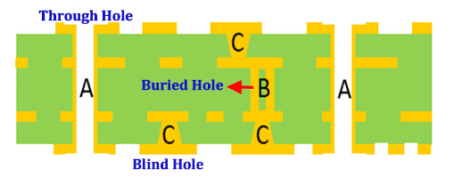
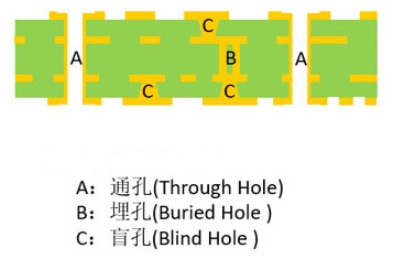
Buried Via vs Blind Via: Understanding Buried Vias in PCB and When to Use Each
The choice between buried via vs blind via hinges on layer connectivity needs. Both are internal vias, but their access points differ.
- Blind Via: Connects an outer layer to an inner layer. Visible on one board surface.
- Buried Via: Connects two or more inner layers without reaching either outer layer. Completely concealed within the board after final lamination.
When to Use Each:
- Use Blind Vias: When you need to connect surface-mounted components (like a BGA) directly to a specific internal signal or power plane. This is the most common scenario for component fanout.
- Use Buried Vias: When you have dense routing between two internal layers that do not require connection to the surface. This helps resolve internal routing congestion without consuming surface real estate or affecting outer layer routing.
The blind via buried via combination is powerful. For example, a design might use blind vias to fan out a BGA to the first inner layer, and then use buried vias in PCB to route between deeper internal layers, maximizing routing efficiency across the entire stack-up.
Step-by-Step Blind Via Process From Drilling to Lamination
The blind via process is more sequential than that for through-hole vias, involving multiple lamination cycles. Here’s a simplified overview for a laser-drilled blind via:
- Core Fabrication: Manufacture the inner layer core that will host the blind via’s target layer.
- Lamination of Build-up Layers: Laminate the dielectric prepreg and copper foil for the outer layer onto the core.
- Laser Drilling: Use a CO₂ or UV laser to ablate the dielectric material down to the target copper landing pad, creating the blind hole meaning in a physical sense.
- Desmear & Cleaning: Remove laser-induced debris and epoxy smear from the hole to ensure good adhesion.
- Electroless Copper Plating: Apply a thin, conductive seed layer to the walls of the hole.
- Electrolytic Copper Plating: Build up the copper thickness to form a robust, conductive barrel—this is how to broach a blind hole electrically.
- Outer Layer Patterning: Apply imaging and etching to define the outer layer circuitry, connecting to the now-plated blind via.
- Final Lamination (if needed): This sub-assembly may be laminated with additional layers, potentially covering it to create a buried via in the final board.
This controlled process is what allows for the creation of reliable, high-density interconnects.
Blind Via vs Backdrill: Electrical and Manufacturing Trade-Offs Explained
Both blind vias and backdrilling are used to mitigate via stub effects and improve signal integrity, especially in high-speed PCB designs. However, the blind via vs backdrill decision reflects two fundamentally different design philosophies: one is designed in from the start, the other is applied as a post-process correction.
Blind Via vs Backdrill
| Aspect | Blind Via | Backdrill |
|---|---|---|
| Core Approach | Stub avoided by design | Stub removed afterward |
| When Applied | During build-up | After full fabrication |
| Via Type | Non-through via | Through-hole via |
| Design Impact | Stack-up planned upfront | Enhances existing design |
| Typical Use | HDI, new designs | Performance retrofit |
A blind via is a proactive solution: the via never creates a long stub because the connection is intentionally limited to specific layers during the initial stack-up design.
Backdrilling, by contrast, is a reactive technique. It removes the unused portion of a through-hole via after fabrication through controlled-depth drilling, improving signal integrity without redesigning the original via structure.
For new high-speed HDI designs, blind vias are typically the more integrated and scalable option.
For existing multilayer designs that require performance improvement without major stack-up changes, backdrilling offers a practical alternative.
How Blind Via Cost Is Calculated and What Drives Pricing Up?
Understanding blind via cost factors is essential for budget-conscious design. The premium over standard through-hole PCBs comes from added process complexity and materials.
Key cost drivers include:
- Additional Lamination Cycles: Each sequence of layers requiring blind vias needs a separate lamination step, increasing press time and handling.
- Laser Drilling: Laser drilling equipment is costly to operate and maintain compared to mechanical drilling. The number of laser shots directly impacts cost.
- Increased Process Steps: Desmear, metallization, and plating of small, high-aspect-ratio holes require precise control and add time.
- Materials: Finer line materials and specialized laser-drillable dielectrics may be required.
- Lower Overall Yield: The complexity of the blind via process can impact production yield, a cost factored into pricing.
Is a via a plated through-hole? While all vias in modern PCBs are plated, not all are through-holes. The blind via hole PCB uses plated blindholes, which require more sophisticated processes than simple through-hole plating, contributing to the cost structure.
Blind Via Hole PCB Applications: Where Blind Via Hole PCB Designs Deliver Real Value
The value of a blind via hole PCB becomes undeniable in applications where performance, density, and reliability converge.
- Mobile Devices & Wearables: Smartphones, tablets, and smartwatches where space is at an absolute premium.
- High-Speed Computing: Servers, network switches, and GPUs requiring excellent signal integrity at multi-gigabit rates.
- Advanced Medical Electronics: Implantable devices and miniaturized diagnostic equipment.
- Aerospace & Defense Avionics: Systems demanding high reliability in compact, rugged packages.
- Advanced Automotive Electronics: ADAS sensors, infotainment, and powertrain control units.
In these fields, the ability to reliably route complex circuits in a small form factor makes blind vias not just an option, but a necessity for successful product development.
To sum up, blind via hole technology is an indispensable enabler for high-density, high-performance PCB design, providing critical connections that save space and enhance signal integrity. This article has explored its definition, benefits, key differences from other via types, manufacturing process, cost considerations, and primary applications.
For designers navigating the complexities of HDI, partnering with an experienced manufacturer is crucial. EBest Circuit (Best Technology) specializes in transforming complex designs into reliable, high-yield production boards. Our expertise in advanced processes like blind and buried vias ensures your product benefits from optimal performance and manufacturability. Pls feel free to contact our engineering team anytime at sales@bestpcb.vn for a consultation.
FAQs
What is the difference between blind via and through-hole via?
- A blind via connects an outer layer to an inner layer without going through the entire board. A through-hole via passes through all layers of the board.
What is the difference between blind and buried via?
- A blind via is visible on one board surface, while a buried via is completely hidden inside the board, connecting only internal layers.
Are blind vias more expensive?
- Yes, due to additional manufacturing steps like laser drilling and sequential lamination, blind vias are more expensive than standard through-hole vias.
What is the difference between blind via and backdrilling?
- A blind via is designed from the start to avoid a long stub. Backdrilling is a secondary operation that removes the stub from an existing through-hole via.
Is a via a plated through-hole?
- In common terminology, a “plated through-hole” (PTH) specifically refers to a via that goes through the entire board. However, all modern vias (blind, buried, micro) have plated holes. So, while all PTHs are vias, not all vias are through-holes.