 language
 english



One-Stop PCBA Manufacturer | Free DFM Check & Fast Turnaround
An unavailable IC, an incorrect BGA footprint, or a delayed PCB shipment can hold up an entire electronics project. When PCB fabrication, component sourcing, and assembly involve separate suppliers, resolving these problems often adds time, rework, and unexpected costs.
Best Technology is a one-stop PCBA manufacturer providing PCB fabrication, electronic component sourcing, SMT/THT assembly, inspection, and functional testing. With over 20 years of manufacturing experience, we support prototypes, small batches, and mass production. Our free DFM check and quick-turn PCBA services help customers identify manufacturing risks before production. But how can you determine whether a supplier can handle your PCB design, quality requirements, and delivery schedule?
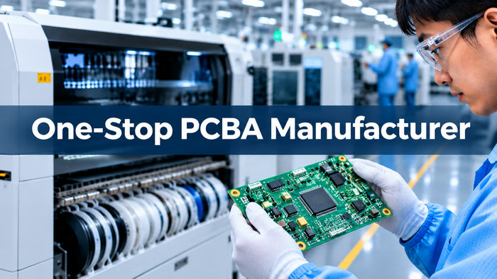
What Does Our One-Stop PCBA Manufacturing Service Include?
Best Technology provides integrated PCB fabrication, component procurement, assembly, inspection, testing, and optional box build services. Customers can manage these manufacturing requirements through one partner instead of coordinating separate PCB and assembly suppliers.
Our one-stop PCBA services include:
- Custom PCB fabrication: FR4 multilayer, flexible, rigid-flex, aluminum, ceramic, and high-frequency PCBs manufactured to approved specifications.
- Electronic component sourcing: Procurement of ICs, resistors, capacitors, connectors, and other components against the approved BOM.
- SMT assembly: Automated placement and reflow soldering for miniature SMD components, QFN, QFP, BGA, and other surface-mount packages.
- Through-hole assembly: Insertion and soldering of connectors, power devices, and other through-hole components.
- Mixed-technology assembly: Integration of surface-mount and through-hole devices on the same PCB.
- PCB inspection and testing: SPI, AOI, X-ray inspection, and electrical or functional testing according to project requirements.
- Box build assembly: Integration of completed PCB assemblies with enclosures, cables, and mechanical components.
Customers can choose three component-supply arrangements:
- Full turnkey PCBA: Best Technology coordinates PCB fabrication, component sourcing, assembly, and the agreed testing scope.
- Partial turnkey PCBA: Customers supply selected components while we source the remaining approved parts.
- Consigned PCBA: Customers provide the agreed components, with PCB fabrication included when required.
These options allow OEM customers to retain purchasing control over critical components without managing every manufacturing stage separately.
What PCB Fabrication and Assembly Capabilities Can We Provide?
Best Technology supports SMT, THT, and mixed-technology assembly, including 01005 SMD components and BGA packages with pitches down to 0.25 mm. Our PCB manufacturing capabilities cover conventional and specialized board constructions used in industrial electronics, medical equipment, communication devices, and other applications.
| Manufacturing Capability | Best Technology Specifications |
|---|---|
| Assembly methods | SMT, THT, mixed assembly |
| Minimum SMD component | 01005 |
| Minimum BGA pitch | 0.25 mm |
| Standard bare PCB size range | 0.2 × 0.2 to 20 × 20 inches |
| Component placement capacity | 13,200,000 chips/day |
| Component packaging | Reel, cut tape, tube, tray, loose parts |
| PCB types | FR4, multilayer, flexible, rigid-flex, metal-core, ceramic, high-frequency |
| Inspection equipment | SPI, AOI, X-ray |
| SMT assembly lead time | 1–5 working days for qualifying orders with materials ready |
Minimum component size and BGA pitch describe process capability, not guaranteed manufacturability for every design. Assembly feasibility also depends on PCB land patterns, solder mask geometry, board flatness, stencil openings, component spacing, and thermal characteristics.
For example, a 0.25 mm pitch BGA requires package-specific review of pad dimensions, solder mask openings, paste application, and any via-in-pad structures. If vias are placed directly within solder pads, their construction and treatment must be compatible with assembly to prevent solder loss and unreliable joints.
Large power components and through-hole connectors introduce different requirements, including soldering access, heat distribution, and mechanical support.
Best Technology reviews the actual PCB and component specifications before confirming assembly feasibility.
How Do We Manage Electronic Component Sourcing and BOM Requirements?
Reliable component sourcing starts with accurate manufacturer part numbers, verified availability, and controlled substitutions. An otherwise manufacturable PCB cannot enter assembly if critical components are missing or incompatible with the approved design.
Best Technology coordinates procurement according to customer-approved BOM requirements.
- BOM verification: Check manufacturer part numbers, quantities, reference designators, package types, and component descriptions.
- Availability assessment: Identify obsolete, unavailable, or long-lead-time components before procurement.
- Approved alternatives: Submit potential replacements for customer engineering approval when the original components cannot be sourced.
- Supplier control: Follow customer restrictions on approved manufacturers, purchasing channels, and component date codes.
- Repeat-order planning: Coordinate material requirements using approved BOM revisions and expected production quantities.
For example, replacing an unavailable voltage regulator requires more than matching its output voltage. The alternative must also satisfy the required input range, load current, pin configuration, footprint, thermal characteristics, and other circuit requirements.
No component substitution proceeds without customer approval. If a replacement affects the PCB footprint or circuit characteristics, engineering verification may be necessary before the assembly can be released.
Early BOM verification also helps identify whether a component is supplied in a suitable format for automated placement, reducing the risk of material shortages or feeding problems when production begins.
How Does Our One-Stop PCBA Manufacturing Process Work?
Our one-stop PCBA manufacturing process connects production-file verification, PCB fabrication, material preparation, assembly, inspection, and testing. Each stage follows the approved manufacturing documents.
Step 1: Manufacturing File Review
Gerber files, fabrication drawings, BOMs, pick-and-place data, and assembly drawings are checked for missing information and inconsistencies.
Step 2: PCB Fabrication and Component Preparation
Bare PCBs are manufactured according to the approved stackup, dimensions, surface finish, and fabrication requirements. Components are prepared against the confirmed BOM.
Step 3: Solder Paste Printing
Solder paste is deposited through a stencil onto the PCB pads. SPI is used when required to evaluate paste deposition before component placement.
Step 4: SMT Placement and Reflow Soldering
Surface-mount components are positioned according to the approved placement data. A controlled reflow process forms the solder joints.
Step 5: Through-Hole Assembly
Connectors, power devices, and other through-hole components are installed using suitable soldering methods. Mixed-technology boards may require additional operations.
Step 6: Inspection and Electrical Testing
Completed assemblies undergo the agreed visual, automated, and electrical inspection procedures. Nonconforming boards are evaluated before acceptance.
Step 7: Final Inspection and Packaging
Accepted assemblies are checked against the required workmanship, identification, and packaging specifications before shipment.
PCB fabrication and assembly are coordinated under one manufacturing order, allowing design clarifications and production changes to be handled without repeated communication between unrelated suppliers.
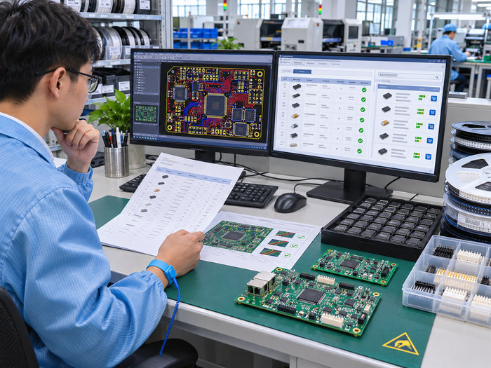
What PCBA Manufacturing Challenges Can We Help You Solve?
Fine-pitch solder defects, BGA joint failures, PCB warpage, and assembly inconsistencies require different engineering responses. Effective troubleshooting starts by identifying where the defect originates rather than repeatedly adjusting the assembly process.
Best Technology helps address the following challenges:
- Fine-pitch solder bridging: Bridging may result from excessive paste, stencil aperture design, component misalignment, or solder mask limitations. The affected pads, paste deposits, placement data, and reflow conditions are reviewed to identify the likely cause before making corrections.
- BGA solder joint defects: Hidden joints cannot be fully inspected optically. Package geometry, PCB land patterns, solder paste requirements, and X-ray findings must be considered together. For high-density BGA designs, via-in-pad construction and board flatness can also affect joint formation.
- PCB warpage during reflow: Warpage may originate from the incoming bare board or develop during thermal processing. Comparing board flatness before and after reflow helps distinguish material or construction problems from assembly-related deformation. Panel support and the thermal process can then be reviewed.
- Mixed SMT/THT soldering problems: Large through-hole connectors, heavy copper areas, and miniature SMT devices respond differently to heat. Component placement, soldering sequence, and thermal requirements are evaluated to select a suitable assembly process.
- Incorrect component orientation: Polarity markings, component datasheets, BOMs, and pick-and-place data must agree. Discrepancies are clarified before assembly, while inspection helps identify placement errors.
- Repeat-production variation: Different PCB revisions, unauthorized component changes, or inconsistent assembly instructions can cause variation between batches. Approved documents and controlled changes help maintain repeatability.
For example, if a BGA assembly shows abnormal X-ray results, replacing the component immediately may not solve the underlying problem. The solder pad geometry, paste deposition, and PCB condition should be evaluated before the next assembly attempt.
The goal is to identify the manufacturing cause, apply an appropriate correction, and prevent the same defect from recurring in subsequent builds.
How Does Our Free DFM Check Help Reduce Manufacturing Defects?
Our free DFM check identifies potential PCB fabrication and assembly problems before materials and production tooling are committed. Customers receive manufacturing feedback that can be reviewed before approving the production files.
The review can cover:
- PCB fabrication features: Trace width, spacing, hole sizes, solder mask clearances, and board-edge requirements.
- Component footprints: Package dimensions, pad geometry, polarity, and consistency between BOM and assembly data.
- Solder paste requirements: Stencil apertures for fine-pitch ICs, QFN thermal pads, and other sensitive packages.
- Assembly accessibility: Component clearances, panel rails, fiducials, and mechanical support requirements.
- Via-in-pad construction: Via placement, filling or capping requirements, and compatibility with the selected component packages.
- Testing accessibility: Test-point locations and access to required electrical interfaces.
What happens when a problem is found?
Best Technology can identify the affected design feature, explain the manufacturing concern, and recommend a correction for customer review.
For example, an unsuitable solder paste opening beneath a QFN thermal pad may increase the risk of component float or soldering defects. The relevant stencil requirement can be reviewed before assembly instead of correcting the issue after soldering.
Manufacturing feedback may identify issues that require correction before production, items needing customer confirmation, and optional improvements to assembly efficiency.
Customers retain approval of all design changes. DFM review evaluates manufacturability and assembly compatibility; it does not replace electrical design verification or product-level validation.
How Do We Ensure PCBA Quality and Reliability?
Best Technology uses incoming inspection, process monitoring, solder joint inspection, and project-specific electrical testing to verify PCBA quality. Inspection methods are selected according to the board construction, failure risks, and agreed acceptance criteria.
Our quality controls include:
- Incoming inspection: Verify received components, packaging, part identification, and material requirements.
- SPI: Check solder paste deposition before placement to identify printing defects.
- AOI: Detect visible assembly defects, including missing components, polarity errors, and selected soldering abnormalities.
- X-ray inspection: Evaluate selected hidden solder joints beneath BGA and other bottom-terminated packages.
- Bare PCB electrical testing: Verify continuity and isolation according to the approved PCB requirements.
- Functional Circuit Testing (FCT): Check specified electrical functions, such as output voltages, sensor signals, or communication interfaces.
- Final inspection: Verify workmanship, identification, and agreed shipment requirements.
Passing AOI or X-ray inspection does not establish that a PCBA functions correctly. An assembly may have acceptable solder joints but still fail because of an incorrect component value, firmware issue, or circuit malfunction.
For an industrial controller, a meaningful functional test might include checking supply rails, verifying digital inputs and outputs, and testing a communication interface under defined conditions.
The customer should establish the required test conditions, pass/fail limits, sampling coverage, and any necessary fixtures before production. Test records and traceability requirements can then be agreed as part of the order.
Our quality management certifications include ISO 9001:2015, ISO 13485:2016, IATF 16949, and AS9100D. Customers with medical, automotive, or aerospace requirements can request the applicable certification documentation and confirm the manufacturing site and scope.
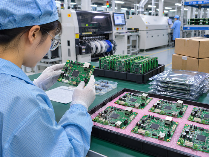
How Do We Support PCBA Prototyping and Batch Production? A Real Manufacturing Case
Best Technology supports prototypes, small-batch PCBA, and mass production through integrated PCB fabrication, component sourcing, assembly, and testing. Prototype builds help identify manufacturing issues, while approved BOMs, production files, and inspection requirements support consistency as quantities increase.
A UK surgical lighting customer ordered 150 assembled LED PCBs plus one spare, requiring aluminum PCB fabrication, component sourcing, and SMT assembly under one manufacturing project.
Project Specifications:
- Application: Surgical lighting equipment
- PCB construction: Single-sided aluminum-core PCB
- Board thickness: 1.6 mm ±10%
- Copper thickness: 1 oz
- Surface finish: Lead-free HASL
- Solder mask: Black
- Order quantity: 150 assemblies plus one spare
Manufacturing Challenges and Solutions:
- LED positioning: The LED array needed to follow the approved optical layout. SMT placement was coordinated with the confirmed component positions.
- Mounting-hole accuracy: Hole locations were critical to fitting the board into the lighting equipment. Optical measurement was used to check the required mounting positions.
- Panel and assembly coordination: The PCB panel and stackup required customer approval before fabrication. PCB manufacturing, component procurement, and SMT assembly were then coordinated within the same order.
- Cleanliness and operation: The assemblies required cleaning, removal of soldering residues, and LED operation checks before shipment.
Project Result: Best Technology completed the PCB fabrication, component sourcing, and SMT assembly project within 1.5 weeks, including the required assembly and inspection work.
The customer received assembled LED boards with mounting and operation checks completed, without having to coordinate separate PCB fabrication, procurement, and assembly suppliers.
This project illustrates our small-batch turnkey manufacturing approach. For larger repeat orders, production quantities and scheduling are confirmed against the approved design, material availability, and testing requirements.
What Is the Typical Lead Time for One-Stop PCBA Manufacturing?
Our SMT assembly lead time is typically 1–5 working days for qualifying orders when bare PCBs, components, and approved production files are ready. This covers the assembly stage, not the entire turnaround time of every full turnkey PCBA project.
For complete turnkey manufacturing, the total lead time also depends on:
- PCB fabrication: Standard FR4 boards and specialized constructions such as HDI, rigid-flex, and ceramic PCBs may require different manufacturing schedules.
- Component procurement: Unavailable ICs, special connectors, and restricted suppliers may extend material preparation.
- Assembly complexity: Double-sided SMT, fine-pitch BGA, and mixed SMT/THT assemblies may require additional processing.
- Testing requirements: Custom functional test fixtures, firmware programming, or special inspection procedures can extend preparation and production time.
- Order quantity: Large or repeat orders require suitable capacity planning and material coordination.
For urgent orders, Best Technology can evaluate quick-turn production after checking the manufacturing files, materials, and available capacity.
The final lead time is confirmed for the complete project scope, including any required fabrication, procurement, assembly, testing, and shipment arrangements.
What Factors Affect One-Stop PCBA Manufacturing Costs?
PCB construction, component selection, assembly complexity, order quantity, and testing requirements determine the main PCBA manufacturing costs. These factors should be reviewed before production because changes made after procurement may create additional work.
The main cost drivers include:
- PCB specifications: Layer count, dimensions, materials, copper thickness, surface finish, and specialized via structures.
- Component requirements: Package type, availability, purchasing restrictions, and handling requirements.
- Assembly operations: Double-sided SMT, fine-pitch components, through-hole soldering, and additional assembly steps.
- Production quantity: Setup and manufacturing efficiency differ between prototypes and repeat production.
- Inspection and testing: X-ray requirements, functional test fixtures, firmware programming, and required documentation.
- Engineering changes: Late BOM revisions or PCB modifications that affect purchased materials or production tooling.
Customers can reduce unnecessary manufacturing costs by:
- Using available, approved components to avoid last-minute sourcing changes.
- Reviewing PCB panelization to improve assembly handling and material utilization.
- Avoiding unnecessary PCB complexity when simpler constructions meet the product requirements.
- Finalizing the BOM and PCB revision before procurement begins.
- Completing DFM review early to reduce preventable rework.
- Defining the required test scope before quotation and fixture preparation.
Cost improvements should not compromise product reliability, specified material requirements, or electrical and mechanical performance.
Why Choose Us as Your One-Stop PCBA Manufacturer?
Best Technology helps OEM customers manage PCB manufacturing risks without coordinating separate fabrication, component sourcing, and assembly suppliers. Founded in 2006, we provide custom PCB and PCBA manufacturing services for industrial electronics, medical equipment, communication products, and other applications.
Our manufacturing support focuses on five customer benefits:
- Identify manufacturing problems before production: Free DFM feedback helps your engineers resolve PCB footprint, solder mask, panelization, and assembly compatibility issues before manufacturing begins.
- Keep critical components under your control: Full turnkey, partial turnkey, and consigned assembly options allow you to manage approved components and retain authority over substitutions.
- Support complex PCB assemblies: SMT capabilities down to 01005 packages and 0.25 mm BGA pitch, together with SMT/THT mixed assembly, cover a broad range of electronic designs subject to feasibility review.
- Reduce coordination across suppliers: PCB fabrication, component sourcing, assembly, and testing requirements are managed within one project, helping prevent mismatched manufacturing information.
- Maintain production continuity: Approved design revisions, material planning, inspection requirements, and project-specific quality documentation support prototype builds and subsequent production orders.
Best Technology can also support projects requiring box build, CNC machining, injection molding, and sheet-metal fabrication.
Whether your priority is solving an assembly problem, qualifying a new manufacturing partner, or preparing a product for repeat production, we can review the manufacturing requirements against your actual PCB design.
FAQs About One-Stop PCBA Manufacturing
Q1: Can Best Technology sign an NDA before receiving confidential PCB files?
A1: Yes. Confidentiality arrangements can be discussed before proprietary design documents are exchanged. Customers may submit their own NDA for review before sharing sensitive manufacturing information.
Q2: How should components that must not be installed be marked in the BOM?
A2: Mark these components as DNP, DNI, or another clearly defined status. The BOM, assembly drawings, and placement data must agree so the correct components are excluded from the assembly.
Q3: What happens if customer-supplied components are insufficient for production?
A3: The supplied quantity is checked against the required assembly quantity and expected handling consumption. If the material is insufficient, the shortage must be resolved before the affected assembly work proceeds. Cut-tape SMT components may require additional feeding allowance.
Q4: Can I change the BOM or PCB revision after an order is confirmed?
A4: Changes can be reviewed, but feasibility depends on the production stage. An updated BOM, PCB revision, placement file, or test requirement may affect purchased materials, tooling, or work in progress. Revised requirements must be approved before implementation.
Q5: Can I approve a first-article assembly before the remaining boards are produced?
A5: Yes, first-article inspection or sample approval can be arranged as part of the agreed production plan. The required checks, acceptance criteria, and approval procedure should be defined before assembly begins.
Q6: How are moisture-sensitive components handled during assembly?
A6: Moisture-sensitive devices are handled according to their moisture sensitivity level, packaging condition, and manufacturer requirements. Appropriate storage, floor-life control, or baking may be necessary depending on component condition and exposure history.
Q7: Can you provide batch traceability and inspection records?
A7: Project-specific component lot information, PCB revisions, inspection results, and test records can be arranged according to agreed requirements. Serial-number-level traceability and document retention periods should be specified before production.
Q8: How are completed PCBA boards packed for international delivery?
A8: Finished boards can be packaged using ESD-protective materials and suitable mechanical protection. Trays, individual packaging, moisture protection, labels, and carton requirements can be arranged according to the product and shipping conditions.
Get a Free DFM Check and Request Your PCBA Quote
Have a PCB assembly project that needs reliable component sourcing, precise SMT assembly, or a faster production schedule? Whether you are preparing your first prototype or transferring an approved design into repeat production, Best Technology can help you identify manufacturing risks before they become delays or rework.
Send your Gerber files, BOM, required quantity, target delivery date, and delivery location to sales@bestpcb.vn. Our team can provide a free DFM check, explain any manufacturing issues that need attention, and prepare a quotation based on your PCB and assembly requirements. Start with a manufacturing review and find out how Best Technology can support your next PCBA project.