 language
 english


Quick Turn Wire Bonding Service for Bare Die, Sensor and PCB Assembly
A wire bonding service connects bare die, sensors and chip pads to a PCB, ceramic substrate or package with fine metal wires. It helps compact products save space, shorten internal connections and support custom chip-on-board assembly.
For a fast project, the most important questions are direct: can the PCB pads be bonded, which wire material should be used, what testing is required and how quickly the assembly can be built. This guide explains the process, materials, cost factors, PCB requirements, quality checks and supplier selection points for custom electronic assembly.
What Is Wire Bonding Service?
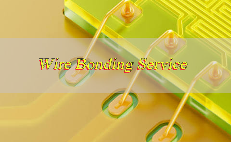
Wire bonding service is a microelectronics assembly process that connects a bare die to a PCB, ceramic substrate, lead frame or package using fine metal wires. These wires create electrical paths between chip pads and external circuit pads.
This process is used when standard packaged ICs are too large, unavailable or unsuitable for the final product structure. It is common in chip-on-board assembly, sensor modules, hybrid circuits, RF devices and compact control electronics.
Unlike normal soldering, the process requires controlled bonding force, ultrasonic energy, heat, pad finish, wire diameter and loop shape. A complete project may include die attach, wire bonding, encapsulation, inspection and final electrical testing.
What Does Wire Bonding Do in Microelectronics Assembly?
A wire bonding service makes a bare chip work inside a complete electronic assembly. It creates fine electrical links between the die and the PCB, substrate or package.
Main functions include:
- Connects chip pads to PCB or substrate pads
- Transfers power, ground and signal paths
- Supports bare die, sensor and chip-on-board assembly
- Reduces package height and board space
- Allows custom IC and sensor integration
- Helps validate samples before batch production
- Supports compact RF, LED, medical and industrial modules
In simple terms, wire bonding turns an unpackaged chip into a working part of the circuit.
What Types of Wire Bonding Services Are Available?
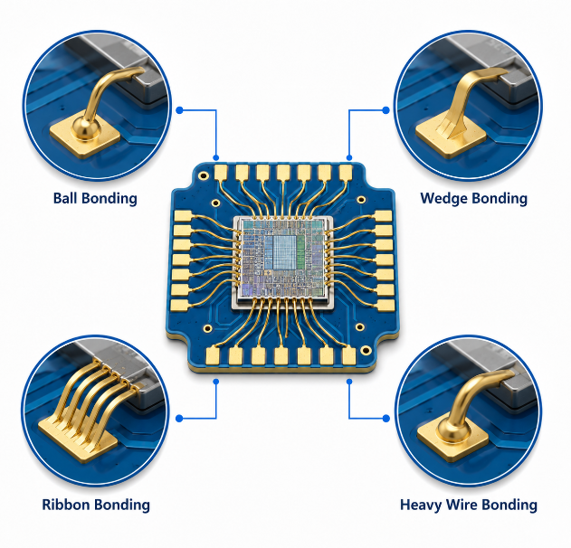
Wire bonding services should be classified by bonding method, not by application name. Ball bonding, wedge bonding, ribbon bonding and heavy wire bonding are process-based service types.
| Type | Wire | Typical Use | Feature |
|---|---|---|---|
| Ball bonding | Gold, copper | Fine-pitch ICs, sensors, COB | Fast and suitable for small pads |
| Wedge bonding | Aluminum, gold | RF, ceramic, power modules | Works well at lower temperature |
| Ribbon bonding | Aluminum, gold | RF and power modules | Lower inductance and higher current path |
| Heavy wire bonding | Aluminum | Power devices, high-current modules | Stronger current handling |
| Fine wire bonding | Gold, copper, aluminum | Bare die IC and sensor assembly | Small wire diameter for dense pads |
A quick turn wire bonding service should review the die pad, PCB finish and bonding diagram before choosing the method. Ball bonding is common for fine-pitch ICs, while wedge bonding is often used for aluminum wire and special substrates.
For small batch bonding projects, tool access, loop direction and inspection method should be confirmed before production. This reduces rework when the sample moves into pilot production.
What Wire Materials Can Be Used for Wire Bonding?
Gold, aluminum, copper and silver are the main wire materials used in wire bonding service projects. The material must match the die pad metal, PCB finish, current load and working environment.
| Material | Typical Size | Feature | Common Use |
|---|---|---|---|
| Gold wire | 17–50 μm | Stable and oxidation-resistant | Fine-pitch ICs, sensors, COB |
| Aluminum wire | 25–250 μm | Cost-effective | Wedge bonding, RF, power |
| Copper wire | 18–50 μm | Strong conductivity | IC packaging, cost-sensitive designs |
| Silver wire | 18–50 μm | Good conductivity | LED and selected IC assembly |
| Aluminum ribbon | 100–500 μm width | High current capacity | Power modules |
Gold wire bonding is often used for fine-pitch ICs, sensors and COB products because gold bonds well and resists oxidation. Aluminum wire bonding is common for wedge bonding, RF modules and power-related designs.
Copper wire can reduce material cost, but it needs tighter process control because it is harder and more sensitive to oxidation. Therefore, the wire material should match the pad metal, surface finish, product environment and reliability target.
What Applications Commonly Use Wire Bonding Service?
Wire bonding service is used when the design needs compact size, direct chip connection or custom bare die integration. It is common in products where standard SMT packages are too large or not available.
Common applications include:
- Bare die IC assembly for engineering samples
- Bare die wire bonding service for custom modules
- Wire bonding service for sensors, MEMS and light-sensing devices
- Chip-on-board control modules
- RF, microwave and antenna modules
- LED, photodiode and laser diode assembly
- Medical monitoring and diagnostic electronics
- Automotive sensor and control modules
- Aerospace and industrial electronics
- Ceramic substrate and hybrid circuit assembly
- Low-volume samples before mass production
What PCB, Substrate and Pad Requirements Are Needed for Wire Bonding?
PCB, substrate and pad design directly affect wire bonding reliability. A PCB wire bonding service needs clean, flat and bondable pads with enough space for the selected wire and bonding tool.
Main requirements include:
- Surface finish: Use ENEPIG, soft gold, bondable gold or another approved finish. Normal solderable finishes may not bond reliably.
- Pad cleanliness: Keep pads free from oxidation, oil, dust, flux residue and fingerprints.
- Pad size: Match pad size to wire diameter, bond foot size and tool access.
- Pad spacing: Leave enough clearance for wire loop, nearby metal and bonding tool movement.
- Solder mask clearance: Keep solder mask away from the bond pad edge to prevent tool interference.
- Pad flatness: Use a smooth, stable bonding area to reduce weak bonds and lifted pads.
- Die attach area: Keep the die placement area flat, clean and mechanically stable.
- Documents: Provide Gerber files, die drawings, pad map, bonding diagram and test requirements.
ENEPIG is often preferred for PCB-based wire bonding because it provides better bondability than many normal PCB finishes. The surface finish should be confirmed before PCB fabrication.
If the PCB finish is wrong, the bonding project may require a new board build. Therefore, pad finish, pad size, solder mask clearance and bonding direction should be checked during DFM review.
How Does the Wire Bonding Process Work Step by Step?
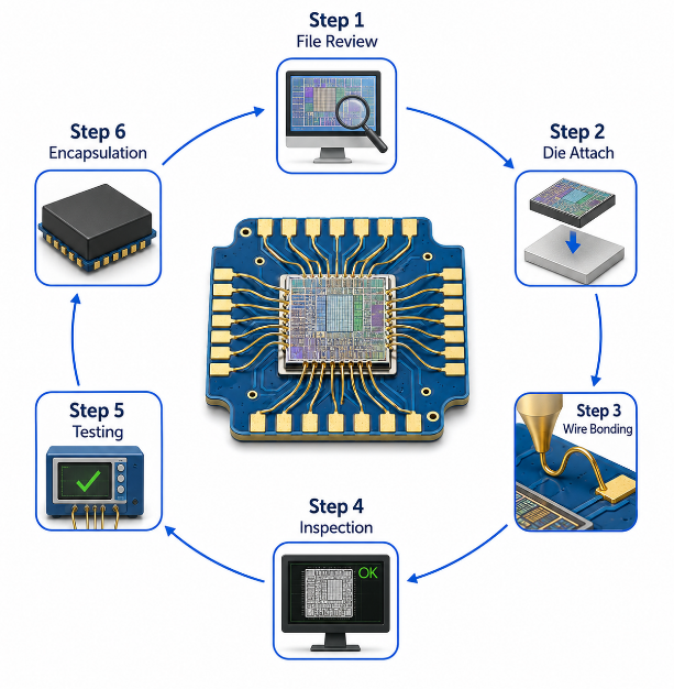
The wire bonding service process starts with file review and ends with testing and protection. Each step must be controlled because small errors can cause weak bonds, lifted pads or broken wires.
Step 1: Review files and bonding requirements.
The team checks Gerber files, die drawings, pad maps, bonding diagrams, BOM, surface finish and testing needs. This confirms whether the PCB pad design and die location are suitable for the selected bonding method.
Step 2: Prepare PCB, substrate and die.
The PCB or substrate is cleaned and inspected. The bare die is checked for correct orientation, pad condition and handling damage before assembly starts.
Step 3: Attach the bare die.
The die is placed on the PCB or substrate with adhesive, solder attach or another approved die attach method. After curing or stabilization, the die must stay flat and secure.
Step 4: Create the wire bonds.
The bonding machine connects each die pad to the matching PCB or substrate pad. The process controls force, ultrasonic energy, bonding time, temperature and loop shape.
Step 5: Inspect the bonded assembly.
Inspectors check wire position, bond shape, loop height, pad condition and possible shorts. Any abnormal wire loop or damaged pad must be reviewed before protection.
Step 6: Test and protect the assembly.
The assembly may receive pull testing, electrical testing, functional testing and encapsulation. Encapsulation protects the die and wires from moisture, dust, handling and vibration.
How Much Does Wire Bonding Cost?
Wire bonding cost is affected by setup work, wire count, die quantity, wire material, bonding difficulty, testing needs and lead time. A simple single-die sample costs less than a fine-pitch multi-die assembly with many wires and special inspection.
For a wire bonding service, setup and engineering review are the first cost factors. A new project may require file review, tooling setup, sample preparation and bonding parameter adjustment. Prototype setup can range from $200–$800, depending on fixture needs and process difficulty.
Wire count also affects price. A design with 10–30 wires is usually faster to bond than a design with 100+ wires. More wires increase machine time, inspection time and the chance of rework.
Material choice matters as well. Gold wire is stable but more expensive. Aluminum wire is cost-friendly for wedge bonding. Copper wire can reduce material cost, but it requires stricter process control.
Testing and protection add cost. Pull testing, shear testing, electrical testing, functional testing and encapsulation may add $50–$300+ per batch, depending on the test plan and quantity.
Quick turn orders can cost more because production time is compressed. For a stable quote, provide die size, pad map, wire count, PCB finish, bonding method, quantity, testing needs and delivery target.
What Is the Alternative to Wire Bonding Service?
Common alternatives to wire bonding service include flip chip bonding, solder bumping, conductive adhesive, TAB bonding and packaged IC assembly. The right choice depends on I/O count, size, current, signal speed, cost and production volume.
| Method | Suitable Project | Advantage | Limitation |
|---|---|---|---|
| Flip chip bonding | High I/O compact modules | Shorter signal path | Higher setup demand |
| Solder bumping | Wafer-level interconnect | Good for volume production | Needs wafer preparation |
| Conductive adhesive | Low-temperature assembly | Gentle on heat-sensitive parts | Lower conductivity than metal |
| TAB bonding | Flexible interconnects | Thin and flexible | Less common for small batches |
| Packaged IC assembly | Standard PCBA | Easier SMT assembly | Larger size than bare die |
| Wire bonding service | Bare die and sensor modules | Flexible for samples and small batches | Wire loop and pad rules must be controlled |
For quick turn bare die samples, wire bonding service is often more practical because it can start with prepared die, a bondable PCB and a clear bonding diagram. Flip chip may be better for very dense, high-speed or high-volume designs.
What Quality Inspection and Testing Are Used After Wire Bonding?
A wire bonding service should be checked through visual inspection, mechanical strength testing, electrical testing and functional verification. The goal is to confirm that each bond is strong, correctly placed and electrically stable.
Common inspection and testing methods include:
- Visual inspection: Checks bond shape, wire loop, pad damage, crossed wires, wire sag and abnormal wire direction.
- Bond pull test: Measures wire bond strength and helps reveal weak bonds.
- Non-destructive pull test: Screens bonds without damaging approved units when required.
- Ball shear test: Checks ball bond adhesion on the pad surface.
- Electrical test: Confirms continuity and checks for opens or shorts.
- Functional test: Confirms the assembled module works under the required operating conditions.
- Encapsulation inspection: Checks coverage, voids, cracks and protection around die and wires.
- Record review: Tracks process settings, inspection results and failure notes for future batches.
For high-reliability products, inspection records help trace whether a failure comes from pad finish, die handling, bonding parameters or assembly design.
What Common Problems Should Be Avoided in Wire Bonding Projects?
Common wire bonding problems include lifted bonds, broken wires, pad peeling, poor adhesion, shorted loops and contamination. Most problems can be reduced when the design is reviewed before PCB production.
Problems to avoid include:
- Wrong PCB finish: Some solderable finishes are not suitable for reliable bonding.
- Dirty pads: Oil, dust, oxidation, flux or fingerprints can weaken adhesion.
- Small pads: A pad that is too small may not hold the bond foot securely.
- Tight spacing: Narrow clearance can cause wire shorts or tool interference.
- Solder mask interference: Mask too close to the pad can block the bonding tool.
- Die tilt: Uneven die attach can create unstable loop height.
- Excessive bonding energy: Too much ultrasonic energy can damage pads.
- Poor wire loop control: Very high or very low loops may break or touch nearby metal.
- Weak encapsulation: Poor protection can allow wire movement, moisture damage or corrosion.
- Unclear bonding diagram: Missing wire path information can cause wrong connections.
The best prevention is early DFM review. Confirm bonding method, pad finish, pad size, wire material, die attach process and inspection plan before the PCB is fabricated.
How to Choose a Quick Turn Wire Bonding Service Provider?
A quick turn wire bonding service provider should help you confirm whether the project can be bonded before production starts. Fast delivery is valuable only when the pad design, die placement, wire material and inspection plan are technically suitable.
A suitable supplier should provide:
- DFM review before PCB fabrication: The supplier should check pad size, pad finish, solder mask clearance, die location and bonding path before boards are produced. This helps avoid rebuilding the PCB because of a wrong finish or pad layout.
- Process matching for the real product: The supplier should recommend ball bonding, wedge bonding, ribbon bonding or heavy wire bonding based on pad metal, wire material, current load and substrate type.
- Wire material guidance: Gold, aluminum, copper and ribbon wire should be matched with the die pad, PCB finish, current requirement and product environment.
- Prototype and small batch support: Quick turn wire bonding services should support sample validation, low-volume trial production and later batch expansion.
- PCB and PCBA coordination: When PCB fabrication, SMT assembly and bonding support are reviewed together, the project has fewer handoff risks and fewer communication gaps.
- Inspection and test support: The supplier should provide visual inspection, pull test, electrical test, functional test or encapsulation inspection according to the project requirement.
- Encapsulation support: If the bonded die and wires need protection from moisture, dust, vibration or handling, the supplier should advise a suitable protection method.
- Clear quotation details: A useful quote should explain setup cost, unit cost, wire material, die quantity, testing scope, MOQ and lead time.
- Practical risk feedback: The supplier should clearly point out possible risks such as wrong pad finish, tight pad spacing, missing bonding diagram or limited spare die.
- Global delivery experience: For overseas custom electronics projects, the supplier should support clear file communication, stable packing and export delivery without claiming fake local factories or warehouses.
Why Choose Best Technology as Wire Bonding Service Provider?
Best Technology helps customers reduce project risk by combining PCB manufacturing, PCBA assembly, engineering review and wire bonding service support from a China-based source factory. This helps customers avoid delays caused by wrong PCB finish, unclear pad design or disconnected suppliers.
Below are reasons why choose Best Technology as wire bonding service provider:
- Fewer handoff risks: PCB fabrication, assembly and bonding support can be reviewed together before production.
- Better pad preparation: We help confirm bondable surface finish, pad size, solder mask clearance and die placement.
- Faster sample progress: Quick turn support helps move bare die and sensor projects from files to working samples.
- Clearer cost control: Early review helps reduce rebuilds, rework and hidden assembly risks.
- Custom project support: We support bare die, sensors, chip-on-board modules, mixed PCBA and small batch projects.
- Inspection support: Visual inspection, electrical checks and project-based testing help improve delivery confidence.
- Global delivery: EBest supplies overseas B2B customers from China with custom PCB, PCBA and assembly support.
If your project involves bare die, sensors, compact modules or special PCB pad requirements, Best Technology can help you review the files before fabrication and reduce avoidable bonding failures.
FAQs About Wire Bonding Service
Q1: What files should be prepared before requesting a quote?
A1: Prepare Gerber files, BOM, die datasheet, die pad map, bonding diagram, assembly drawing and test requirements. If the die is supplied in wafer form, include wafer map and dicing details. Complete files help confirm pad finish, wire count, bonding path and assembly risk before quoting.
Q2: Can customer-supplied bare die be used?
A2: Yes, a wire bonding service can use customer-supplied bare die if it is clean, traceable and safely packed. The supplier should confirm die quantity, die orientation, pad condition, storage condition and handling method before assembly. Extra sample die should be prepared for setup, inspection and possible process adjustment.
Q3: Does wire bonding require a special PCB surface finish?
A3: Yes, the PCB finish must be bondable. ENEPIG, soft gold and approved bondable gold finishes are commonly used. Standard soldering finishes may not provide stable adhesion. The surface finish should be confirmed before PCB production because a wrong finish may require a new board build.
Q4: Can a wire bonded assembly be protected after bonding?
A4: Yes, encapsulation can protect the die and wires after bonding. Epoxy or other approved material can reduce damage from dust, moisture, touch, vibration and handling. The encapsulation material should match the product environment, inspection needs and future repair requirements.
Q5: How many extra die should be prepared for a prototype run?
A5: It is safer to prepare extra die for setup and inspection. For a small prototype run, prepare at least 10%–30% extra die, depending on die cost, bonding difficulty and test requirements. Fine-pitch or fragile die may need more spare units.
Q6: Can wire bonding support very small batch orders?
A6: Yes, a wire bonding service can support small batch and prototype orders. The unit cost is higher for small quantities because setup, review and machine preparation are shared across fewer units. Small batches are useful for proving circuit function before larger production.
Q7: Why do some wire bonded PCBs have a black epoxy cover?
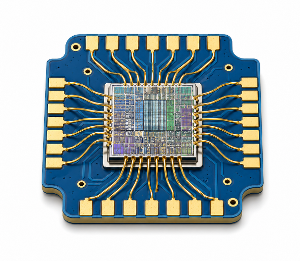
A7: The black epoxy cover usually protects a chip-on-board assembly. A bare die is attached to the PCB, connected with fine wires and covered with epoxy. This protects the die and wire loops from moisture, dust, handling damage and vibration during use.
Q8: Can wire bonding be used for high-current applications?
A8: Yes, but the design may need heavy aluminum wire, ribbon bonding, wider pads or multiple wires in parallel. Current capacity depends on wire material, wire size, wire length, pad strength and heat dissipation. High-current projects should be reviewed before PCB fabrication.
Q9: Can wire bonding be repaired or reworked?
A9: Some wire bonds can be reworked if the pad is still clean, undamaged and large enough for another bond. Rework is risky for fine-pitch die pads because repeated bonding can damage the pad surface. Clear bonding diagrams and inspection reduce rework risk.
Q10: How should bonded assemblies be packed for shipment?
A10: Bonded assemblies should be packed with anti-static protection, tray separation, moisture control and mechanical support. Wires and die areas should not be touched or pressed. If the assembly is not encapsulated, packaging protection becomes even more important during transport.
Q11: Is wire bonding suitable for medical or automotive electronics?
A11: Wire bonding can be used in medical and automotive electronics when the design, material, process and inspection requirements are controlled. These projects may need stricter documentation, stronger process records, functional testing and better protection against vibration, moisture and temperature stress.
Q12: What causes intermittent signals in a wire bonded assembly?
A12: Intermittent signals may come from weak bonds, cracked pads, broken wires, contamination, unstable die attach or poor encapsulation. The problem may appear only during vibration, temperature change or handling. Inspection records and electrical testing help locate the failure source faster.
Conclusion
Reliable wire bonding depends on the correct wire material, bondable pad finish, clean substrate, controlled process and proper inspection. For bare die, sensor, chip-on-board and compact PCB assembly projects, wire bonding service gives a flexible path from custom design to working samples.
If your project needs bare die bonding, sensor assembly, PCB pad review, prototype support or small batch production, send your files to us for a fast technical review. Best Technology supports custom PCB, PCBA and wire bonding service project coordination from China with global delivery. Contact Best Technology via sales@bestpcb.vn today and get a clear quotation for your next project.