 language
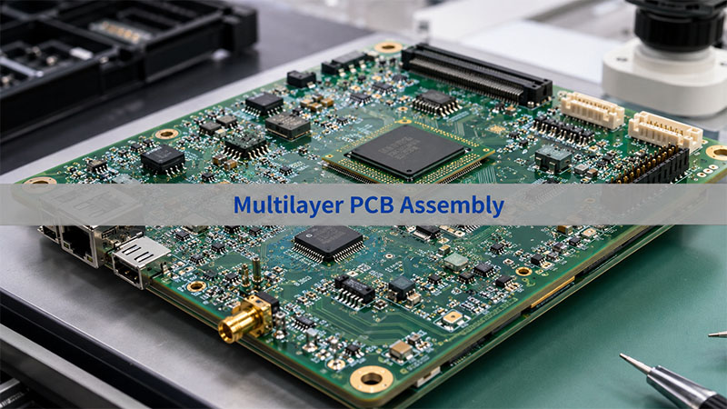
Multilayer PCB Assembly | Process, Design Support & Custom Manufacturing
Multilayer PCB assembly turns a multi-layer circuit board into a working electronic product. It includes PCB fabrication, component sourcing, SMT assembly, through-hole assembly, inspection, testing, and final delivery.
For simple boards, the process is often easy to manage. However, multilayer boards need more care. They may include BGA chips, fine-pitch ICs, dense routing, high-speed signals, and power circuits. Because of this, the project should be checked before production starts.
A good PCBA partner should not only mount parts on a board. It should also check the design, review the BOM, control soldering quality, and test the final product. As a result, customers can reduce risk before mass production.
Best Technology provides one-stop PCB and PCBA manufacturing support from its Vietnam PCBA factory. We support DFM review, BOM sourcing, SMT assembly, AOI inspection, X-ray inspection, functional testing, and production follow-up. For project review or quotation support, please contact sales@vn.danyupcbs.com.
What Is Multilayer PCB Assembly?
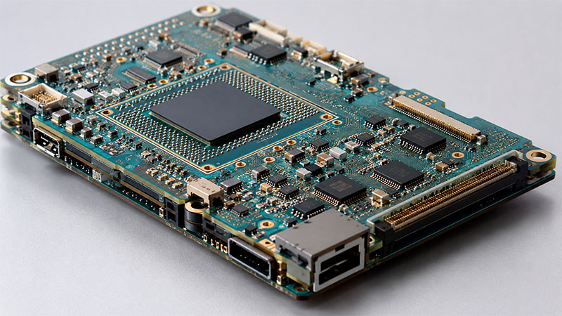
Multilayer PCB assembly is the process of placing and soldering electronic parts onto a PCB with three or more copper layers. These boards may include signal layers, ground layers, power layers, plated holes, blind vias, buried vias, or HDI structures.
In many products, multilayer boards help save space. They also allow more signals to fit inside a smaller board. Therefore, they are widely used in industrial control, medical electronics, communication devices, automotive electronics, UAVs, robotics, new energy products, and instruments.
First, the Bare PCB Must Be Made Correctly
Before assembly starts, the bare PCB must be built well. This step may include inner layer imaging, etching, lamination, drilling, copper plating, solder mask, surface finish, and electrical testing.
If the bare board has problems, assembly becomes harder. For example, poor via plating may reduce reliability. Also, an uneven surface finish may affect soldering. In addition, a wrong stack-up may affect signal quality.
Therefore, PCB fabrication must be controlled from the start.
Then, PCBA Assembly Makes the Board Work
After the bare PCB is ready, the assembly process begins. This stage includes solder paste printing, SMT placement, reflow soldering, through-hole insertion, AOI inspection, X-ray inspection, functional testing, and final quality control.
Compared with double-sided PCB assembly, multilayer PCBA needs tighter control. The board often has more parts, smaller pads, closer spacing, and higher quality needs.
Best Technology treats PCB fabrication, component sourcing, and PCBA assembly as one complete project. As a result, customers can reduce communication gaps and move faster from prototype to production.
What Design Challenges Do Multilayer PCBs Face Before Assembly?
A multilayer PCB may look correct in design software. However, it still needs to match real production rules. This is why DFM, DFA, and DFT review are important before manufacturing.
DFM means design for manufacturing. DFA means design for assembly. DFT means design for testing. Together, these checks help improve yield, reduce rework, and make testing easier.
Stack-Up Design
The stack-up affects signal quality, power stability, and cost. For high-speed circuits, it can also affect impedance.
So, engineers should review the layer order before production. They should also check copper thickness, dielectric thickness, signal layers, ground layers, and power layers.
A clear stack-up helps the board perform better. Moreover, it helps the factory control production with fewer surprises.
Via Placement
Vias are important in multilayer boards. However, poor via placement can create soldering issues.
For example, an open via near a pad may pull solder away from the joint. Also, via-in-pad design may need filling and plating if the board uses BGA chips.
For BGA parts, via design is even more important. Therefore, the team should check pad size, via-in-pad design, solder mask opening, and routing space before production.
Test Points and Panel Design
Testing should be planned early. If the board has too few test points, final testing becomes harder. Also, repair and fault finding may take more time.
Panel design also matters. A good panel should include rails, fiducials, tooling holes, and a clear breakaway method. As a result, SMT production can run more smoothly.
Key Review Points Before Assembly
| Design Area | Common Risk | Review Focus |
|---|---|---|
| Stack-up | Poor signal quality | Layer order, copper thickness, reference plane |
| Vias | Solder loss or routing issue | Via-in-pad, blind vias, buried vias |
| BGA layout | Hidden solder defects | Pad size, fanout, X-ray access |
| Component spacing | Solder bridge or repair difficulty | Fine-pitch ICs, connectors, tall parts |
| Thermal design | Local hot spots | Thermal vias, copper balance, heat path |
| Test points | Low test coverage | ICT points and functional test access |
| Panelization | Low SMT efficiency | Rails, fiducials, tooling holes, V-cut |
Best Technology helps customers review Gerber files, BOM, pick-and-place files, assembly drawings, and test needs before production. In this way, many issues can be found early.
How Does the Multilayer PCB Assembly Process Work from Fabrication to Testing?
A strong assembly process follows clear steps. Each step supports the next one. For example, BOM review helps avoid material delays. Also, DFM review helps reduce production problems.
Step-by-Step Process
| Step | Process | Purpose |
|---|---|---|
| 1 | File review | Check Gerber, BOM, CPL, drawings, and notes |
| 2 | DFM and DFA check | Find risks before production |
| 3 | Component sourcing | Prepare ICs, passives, connectors, and special parts |
| 4 | PCB fabrication | Build the multilayer bare board |
| 5 | Incoming inspection | Check PCB and component quality |
| 6 | Solder paste printing | Apply paste to SMT pads |
| 7 | SMT placement | Mount parts accurately |
| 8 | Reflow soldering | Form stable solder joints |
| 9 | AOI inspection | Check missing parts, offset, polarity, and solder defects |
| 10 | X-ray inspection | Check BGA, QFN, and hidden solder joints |
| 11 | Through-hole assembly | Assemble connectors, terminals, relays, or large parts |
| 12 | Functional testing | Check board performance |
| 13 | Final inspection | Confirm quality before shipment |
Why Process Control Matters
Multilayer PCBA projects often use costly ICs and compact layouts. Therefore, process control helps protect both quality and cost.
For example, a stable reflow profile improves solder joints. AOI can find visible defects quickly. Meanwhile, X-ray inspection can check hidden joints under BGA and QFN parts.
Best Technology supports this workflow in its Vietnam PCBA factory. From file review to final inspection, our team keeps the process clear and controlled.
What Assembly Difficulties Arise with Multilayer PCBs and How Does Best Technology Ensure Quality?
Multilayer boards often carry more functions in less space. As a result, assembly needs higher accuracy and stronger inspection.
Fine-Pitch Components
Fine-pitch ICs need accurate solder paste and stable placement. If there is too much paste, solder bridges may form. If there is too little paste, the solder joint may become weak.
To reduce this risk, Best Technology reviews stencil design, pad layout, component spacing, and placement needs before assembly.
BGA and Hidden Solder Joints
BGA solder joints sit under the component. So, visual inspection is not enough. X-ray inspection helps check solder ball position, voids, shorts, and open joints.
For BGA-heavy boards, this step is very useful. It gives customers more confidence in quality.
PCB Warpage
Some multilayer boards may bend during reflow. This can happen when the board is large, thin, or has uneven copper. Warpage may affect BGA soldering and connector alignment.
Because of this, Best Technology checks board structure, panel design, copper balance, and reflow control when needed.
Mixed SMT and Through-Hole Assembly
Many products use both SMT and through-hole parts. These may include connectors, terminals, transformers, switches, relays, or large capacitors.
In this case, the assembly order matters. Best Technology plans the process to support clean soldering and stable inspection.
Quality Control Methods
Best Technology uses several quality control steps for multilayer PCBAs:
- DFM review before production
- Incoming inspection for PCBs and components
- Solder paste printing control
- SMT placement inspection
- AOI inspection
- X-ray inspection for hidden joints
- Functional testing based on customer needs
- Final inspection before packing
Through these controls, customers can reduce quality risks and improve repeat orders.
How Does Best Technology Solve Signal Integrity and Reliability Issues in Multilayer PCB Assembly?
Signal quality is one main reason engineers use multilayer PCBs. A good layer structure can improve grounding, reduce noise, and support high-speed signals. Still, the final result also depends on fabrication and assembly quality.
Controlled Impedance and Ground Layers
High-speed circuits often need controlled impedance. Common examples include Ethernet, USB, HDMI, LVDS, MIPI, PCIe, and RF circuits.
For these boards, the stack-up should match the design target. Copper thickness, dielectric thickness, and reference layers must work together. Also, stable ground layers help reduce noise.
Via Control and High-Speed Routing
Vias can affect signal quality. For high-speed circuits, via size, via length, and via location should be reviewed.
When needed, Best Technology can help check key manufacturing points before production. This helps reduce signal loss, noise, and unstable performance.
Thermal Reliability
Many multilayer PCBAs include power devices, LED drivers, regulators, motor control ICs, or communication chips. These parts may create heat during use.
Good thermal design helps improve product life. For example, engineers may use thermal vias, thicker copper, larger copper areas, or better materials. Best Technology can review these points during the early project stage.
Testing and Traceability
Reliability also depends on inspection and testing. Therefore, Best Technology supports AOI, X-ray inspection, electrical checks, and functional testing based on project needs.
For industrial control, medical electronics, communication devices, UAVs, and new energy products, this process helps support stable product performance.
What Materials, Stackups, and Surface Finishes Are Best for Multilayer PCB Assembly?
The right material depends on the product. Some projects need lower cost. Others need better heat resistance, better signal quality, or compact routing.
Common PCB Materials and Structures
| Option | Typical Use | Main Benefit |
|---|---|---|
| Standard FR-4 | General electronics and control boards | Good cost and stable performance |
| High-Tg FR-4 | Industrial, automotive, and power boards | Better heat resistance |
| HDI stack-up | Compact and BGA-heavy designs | Higher routing density |
| Flexible multilayer PCB | Compact or bendable products | Flexible connection |
| Rigid-flex PCB | Complex product structures | Fewer connectors and better integration |
FR-4 is widely used because it offers stable performance at a practical cost. However, High-Tg FR-4 may be better for products that face higher heat or lead-free reflow stress.
For compact products, HDI boards support smaller vias and higher routing density. Meanwhile, flexible and rigid-flex boards help save space and reduce connector use.
Surface Finish Options
| Surface Finish | Suitable For | Main Advantage |
|---|---|---|
| ENIG | BGA, fine-pitch ICs, high-reliability boards | Flat surface and good solderability |
| ENIG 2U | Selected projects with thicker gold needs | Better surface reliability for special use |
| OSP | Cost-sensitive SMT boards | Flat and economical |
| HASL | Standard boards with larger pads | Lower cost |
| Immersion silver | RF and high-speed boards | Good electrical performance |
ENIG is often a strong choice for multilayer PCBA. It supports fine-pitch parts and BGA assembly. Still, the final choice should match the design, storage time, soldering process, and budget.
Best Technology helps customers choose suitable materials and finishes based on real project needs. This makes production easier and more stable.
How Does Best Technology Support Prototype, Quick Turn, and Custom Multilayer PCB Assembly?
Prototype speed matters in product development. A late sample can delay firmware testing, mechanical testing, certification work, and customer approval. Therefore, quick and reliable prototype support is very useful.
Prototype Assembly Support
Best Technology supports engineering samples and small-batch builds. Before production starts, our team can review Gerber files, BOM, pick-and-place files, and assembly notes.
This review helps customers find issues early. For example, the team may check part availability, pad design, part polarity, soldering risk, or test access.
Quick Turn PCBA Support
For urgent projects, Best Technology can coordinate PCB fabrication, component sourcing, SMT assembly, inspection, and shipment planning.
Because our Vietnam PCBA factory supports integrated production, customers can reduce supplier coordination time. Also, our team can communicate with customers during the build. This keeps the project moving.
Custom Multilayer PCB Assembly
Different products need different assembly plans. Some boards include HDI structures. Others use BGA, fine-pitch ICs, high-current circuits, RF areas, or mixed SMT and THT parts.
Best Technology supports custom multilayer PCBA based on customer drawings, BOM, test needs, and production goals.
Turnkey PCBA Service
For customers who want one supplier to handle the full project, Best Technology offers turnkey PCBA support. This can include PCB fabrication, component sourcing, SMT assembly, through-hole assembly, testing, final inspection, and packing.
As a result, customers can save time and reduce communication work.
Why Choose Best Technology as Your Multilayer PCB Assembly Manufacturer?
Choosing a multilayer PCB assembly manufacturer is not only about price. A strong supplier can help reduce risk, improve quality, shorten project time, and support long-term production.
Best Technology provides PCB and PCBA manufacturing support from its Vietnam PCBA factory. We help customers move from prototype to production with engineering review, sourcing support, assembly, inspection, and testing.
One-Stop PCB and PCBA Manufacturing
Best Technology supports PCB fabrication, component sourcing, SMT assembly, through-hole assembly, testing, and final delivery. This one-stop model keeps the project clear and organized.
Instead of working with many vendors, customers can manage the PCBA project through one team. This improves communication and reduces handover errors.
Vietnam PCBA Factory for Global Customers
Our Vietnam PCBA factory supports overseas customers who need stable quality, practical lead time, and fast communication. It is a good choice for companies looking for electronics manufacturing support in Vietnam.
For customers in North America, Europe, Southeast Asia, and other regions, Vietnam PCBA production can support supply chain flexibility.
DFM Review and BOM Optimization
Many PCBA problems start before production. For example, the BOM may include obsolete parts, long-lead-time parts, wrong package sizes, or unclear part numbers.
Best Technology can review the BOM and suggest practical options when needed. In addition, our engineering team can check DFM and DFA risks before assembly starts.
Inspection and Testing Capability
For multilayer boards, inspection is important. Best Technology can support AOI inspection, X-ray inspection, electrical checks, and functional testing based on the project.
These steps are useful for boards with BGA, QFN, fine-pitch ICs, dense layouts, and strict quality needs.
Experience with Demanding Industries
Best Technology has experience supporting customers in industrial control, medical electronics, communication, automotive electronics, aerospace/UAV, LED lighting, new energy, robotics, and instruments.
These industries often need stable quality, clear documents, traceability, and process control. Therefore, our team focuses on both engineering review and production execution.
Clear Communication and Quote Support
Good communication can save time. Best Technology supports English communication and practical engineering feedback.
For a quote, please prepare your Gerber files, BOM, pick-and-place file, assembly drawing, testing requirements, and target quantity. Then send them to sales@vn.danyupcbs.com. Our team will review your project and provide support.
To sum up, multilayer PCB assembly needs careful planning. It is not only about soldering parts onto a board. It also includes design review, material selection, BOM checking, SMT control, inspection, testing, and delivery management.
For boards with BGA, HDI routing, fine-pitch ICs, controlled impedance, or high reliability needs, early engineering support can make production smoother. It can also reduce delays, rework, and quality risks.
Best Technology supports global customers with one-stop multilayer PCB assembly services from its Vietnam PCBA factory. Whether your project is a prototype, small batch, or production order, our team can review files, source components, assemble boards, inspect quality, and support testing.
For project review or quotation support, pls feel free to contact us at sales@vn.danyupcbs.com.
FAQs About Multilayer PCB Assembly
1. What is multilayer PCB assembly?
Multilayer PCB assembly is the process of placing and soldering components onto a PCB with three or more copper layers. It usually includes PCB fabrication, component sourcing, SMT assembly, through-hole assembly, inspection, testing, and delivery.
2. What files are needed for multilayer PCB assembly quotes?
You should provide Gerber files, BOM, pick-and-place file, assembly drawing, PCB specifications, test requirements, quantity, and special notes. These notes may include impedance control, surface finish, coating, or packing needs.
3. How much does multilayer PCB assembly cost?
The cost depends on board size, layer count, material, surface finish, component quantity, SMT points, BGA parts, testing needs, lead time, and order quantity. So, a custom quote is more accurate than a fixed price list.
4. Can Best Technology support quick turn multilayer PCB assembly prototypes?
Yes. Best Technology supports prototype and small-batch multilayer PCBA from its Vietnam PCBA factory. We can help with file review, BOM checking, component sourcing, SMT assembly, inspection, and testing.
5. Is ENIG suitable for multilayer PCB assembly?
Yes. ENIG is often suitable for multilayer PCB assembly, especially when the board has BGA, fine-pitch ICs, or small pads. It offers a flat surface and good solderability.
6. What is the difference between multilayer PCB assembly and double-sided PCB assembly?
Double-sided PCB assembly uses circuits on two sides of the board. Multilayer PCB assembly uses boards with three or more copper layers. Because of this, multilayer boards can support denser routing, better signal control, and more complex functions.
7. How does Best Technology inspect BGA solder joints?
BGA solder joints are hidden under the component. Therefore, visual inspection is limited. Best Technology can use X-ray inspection to check solder ball position, voids, shorts, and open joints.
8. Can multilayer PCB assembly support HDI, flexible, and rigid-flex boards?
Yes. Multilayer PCB assembly can support HDI boards, flexible multilayer boards, and rigid-flex PCBs. However, the design, material, stack-up, and assembly process should be reviewed early.
9. How do I choose a reliable multilayer PCB assembly manufacturer?
Look for a supplier with PCB fabrication knowledge, SMT assembly capability, DFM support, BOM sourcing ability, AOI and X-ray inspection, testing support, clear communication, and prototype-to-production experience. Best Technology provides these services through its Vietnam PCBA factory.