 language
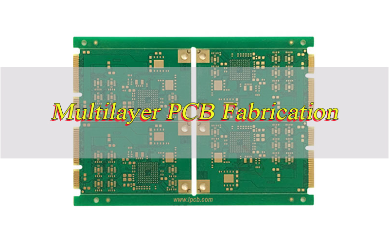
Best Multilayer PCB Fabrication Manufacturer in China, Free DFM
Are you seeking a reliable multilayer PCB fabrication partner? Many professionals face challenges with complex workflows, quality lapses, and delays when sourcing multilayer PCBs. This blog outlines core definitions, fabrication processes, common challenges, and manufacturer selection criteria to help you make informed decisions.
What is Multilayer PCB Fabrication?
Multilayer PCB fabrication involves manufacturing printed circuit boards with three or more conductive layers, each separated by insulating substrates. Layers are bonded via controlled heat and pressure, with plated through-holes (vias) enabling electrical connectivity across the board.
Unlike single or double-sided PCBs, multilayer PCBs offer higher component density, better signal integrity, and space efficiency, critical for complex electronics. Fabrication requires precise layer alignment, strict insulation control, and accurate via plating for reliability.
It is essential for modern electronics (smartphones, medical devices, automotive systems, AI servers) where miniaturization and high performance are required. Growing device complexity increases demand for high-quality multilayer PCB fabrication, driving manufacturers to refine advanced technologies and standards.
What is the Multilayer PCB Fabrication Process?
Multilayer PCB fabrication follows a precise sequence of steps, each requiring strict control to avoid defects and meet specifications:
- Substrate Preparation: Select high-quality insulating substrates (typically industry-standard FR4), cut to size, and clean to remove contaminants that compromise bonding or conductivity.
- Copper Cladding: Coat both substrate sides with a thin, uniform copper layer (electrolytic or electroless plating) to serve as the conductive circuit base.
- Photoresist Application: Apply a photosensitive photoresist to the copper-clad substrate; it hardens under UV light to transfer the circuit pattern.
- Circuit Patterning: Place a photomask (with the desired circuit pattern) over the substrate, expose to UV light, remove unhardened photoresist, and expose the copper circuit pattern.
- Etching: Remove exposed copper with a chemical solution, strip remaining photoresist, and clean the circuit layer for lamination.
- Lamination: Stack circuit layers with insulating substrates, bond via heat and pressure in a lamination press (calibrated to avoid circuit damage).
- Drilling: Drill precise vias through the laminated board to connect different layers, as their size and position directly impact electrical performance.
- Plating: Plate vias with copper to create a continuous conductive path across all layers.
- Solder Mask Application: Apply a solder mask to protect copper circuits from corrosion, short circuits, and solder bridging during assembly.
- Silkscreen Printing: Print a silkscreen layer over the solder mask to label components and test points for easier assembly and maintenance.
- Testing and Inspection: Conduct rigorous tests (continuity, insulation resistance, visual) to detect defects like cracks, voids, or misaligned layers.
What Are Common Challenges in PCB Multilayer Fabrication & How We Solve Them?
Multilayer PCB fabrication’s complexity can lead to defects; below are common challenges and our solutions:
- Layer Alignment Issues: Misaligned layers cause short circuits or poor connectivity, especially in high-layer-count PCBs. We use advanced alignment equipment with high-precision cameras and automated positioning, marking layers with alignment targets and calibrating presses to ±25μm accuracy (misalignment rate <0.1%).
- Via Plating Defects: Uneven plating, voids, or poor adhesion cause signal loss or failure. We use vertical continuous plating (VCP) with pulse plating for uniform copper thickness and 100% X-ray via inspection to detect defects early.
- Impedance Control Inconsistencies: Inconsistent impedance degrades high-frequency signals. We use substrates with stable dielectric constants, precise line width/spacing control, and time-domain reflectometry (TDR) to ensure ±5% tolerance.
- Lamination Voiding: Voids reduce structural integrity and cause delamination. We use vacuum lamination with stepped temperature/pressure profiles and pre-bake substrates/prepreg to remove moisture (a key void cause).
- Etching Unevenness: Uneven etching harms electrical performance. We use automated equipment with precise chemical/temperature control, monitoring in real time to ensure uniform copper removal.
Why Choose Best Technology as Your Multilayer PCB Fabrication Manufacturer in China?
Here are why choose us as your multilayer PCB fabrication manufacturer in China:
- Free DFM Services: Free design for manufacturability (DFM) reviews identify design issues pre-fabrication, with recommendations to optimize line widths, via placement, and materials.
- 20+ Years of Industry Experience: Decades of expertise in PCB multilayer fabrication, handling thousands of projects across automotive, medical, consumer electronics, and aerospace.
- Strict Quality Control Standards: Adhere to IPC-A-600 and ISO 9001, with full-process monitoring and testing to ensure PCB reliability and performance.
- Competitive Pricing: Transparent, competitive pricing via local supply chains and efficient processes, no hidden fees.
- Flexible Production Capabilities: Support small-batch prototypes (MOQ 1) and large-volume production to test designs before scaling.
- Fast Turnaround Times: 5-7 days for prototypes, 10-15 days for mass production, with expedited options for urgent orders.
- Global Customer Support: 24/7 support with technical assistance for design, production updates, and post-delivery needs.
What Types of Multilayer PCB Fabrication Services Do We Offer?
We offer comprehensive multilayer PCB fabrication services for diverse industries, including:
- Multilayer FR4 PCB Fabrication: Industry-standard FR4 PCBs (4-32 layers, 0.5oz-6oz copper, up to 600x800mm) for consumer electronics, industrial controls, and telecommunications.
- Multilayer HDI PCB Fabrication: High-density interconnect (HDI) PCBs (0.1mm microvias, 3/3mil line width/spacing, up to 24 layers) for miniaturized devices like smartphones and medical equipment.
- Multilayer LTCC Ceramic PCB Fabrication: Low-temperature co-fired ceramic (LTCC) PCBs (up to 16 layers, 0.1mm-1.0mm ceramic) for high-temperature/high-frequency aerospace, defense, and automotive applications.
- Multilayer Rigid-Flex PCB Fabrication: Rigid-flex PCBs (up to 12 layers, polyimide flexible sections, FR4 rigid sections) for wearables, automotive sensors, and medical devices.
- Multilayer Heavy Copper PCB Fabrication: Heavy copper PCBs (2oz+ copper, up to 16 layers) for power supplies, industrial equipment, and automotive electronics.
How Do We Control the Quality of Multilayer PCB Fabrication?
To ensure our multilayer PCBs meet industry standards and your requirements, we implement a rigorous full-process quality control system. Our key measures include:
- Incoming Material Inspection: We strictly inspect all raw materials—including substrates, copper foil, prepreg, and solder mask—before they enter the production line. We test key properties such as dielectric constant, copper thickness, and thermal stability to ensure they meet IPC and ISO standards, rejecting any defective materials to eliminate potential quality risks from the source.
- Process Control Monitoring: Every critical step of multilayer PCB fabrication is monitored in real time using advanced equipment. We closely track temperature, pressure, chemical concentration, and etching time, with automated alerts to detect any deviations from standard processes. Immediate corrective actions are taken to ensure consistency and accuracy throughout production.
- Automated Testing Equipment: We utilize state-of-the-art automated testing tools to leave no room for defects. X-ray inspection checks via quality and layer alignment, flying probe testing verifies continuity and insulation resistance, and AOI (automated optical inspection) detects surface defects such as scratches, voids, or misaligned components efficiently.
- Quality Audits and Certifications: We conduct regular quality audits to ensure full compliance with international standards including IPC-A-600, ISO 9001, and ISO 13485. Detailed records of all production and testing activities are maintained for full traceability, which is crucial for industries like medical and automotive.
- Final Inspection: Before shipment, every finished PCB undergoes a comprehensive visual and electrical inspection. Our team checks for physical defects, verifies electrical specifications against your design requirements, and ensures compliance with relevant standards, only PCBs that pass all tests are delivered to you.
How Do We Ensure On-Time Delivery for Multilayer PCB Fabrication Orders?
Our approach to reliable on-time delivery for multilayer PCB fabrication orders:
- Advanced Production Planning: We use professional automated production planning software to optimize our manufacturing schedules. The software comprehensively considers order priority, production capacity and real-time material availability, ensuring each multilayer PCB fabrication order is arranged efficiently and reasonably.
- Efficient Production Processes: We have invested in advanced automated production equipment, which effectively reduces production bottlenecks and ensures a smooth workflow from substrate preparation to final inspection, improving the efficiency of multilayer PCB fabrication.
- Real-Time Order Tracking: We provide an online order tracking portal, allowing you to monitor the real-time status of your multilayer PCB fabrication order at any time and receive timely updates if there is any potential delay.
- Expedited Production Options: For urgent orders, we offer expedited production services, with a turnaround time of 24-48 hours for small-batch prototypes, and we prioritize these orders and allocate additional resources to ensure on-time delivery.
- Reliable Logistics Partnerships: We cooperate with leading logistics providers, offering express, air and sea freight options to meet your different delivery needs, and each multilayer PCB is carefully packaged to avoid damage during transit.
Case Studies of Our Multilayer HDI PCB Fabrication for Home Appliances
A detailed case study of our multilayer HDI PCB fabrication for smart refrigerators:
Project Background: A leading home appliance manufacturer needed high-quality multilayer HDI PCBs for their new smart refrigerators, which rely on PCBs for core functions like remote temperature control and Wi-Fi connectivity. Their previous supplier caused issues with inconsistent quality, delivery delays, and poor signal performance, threatening their product launch.
Project Requirements: The project required 12-layer HDI PCBs with 0.15mm microvias, 4/4mil line width/spacing, 170℃ high-Tg FR4 substrate, and an 80x100mm form factor. They needed to support stable Wi-Fi, operate at 0-40℃, comply with IPC-A-600 Class 2, with 7-day prototypes and 15-day mass production (10,000 units).
Our Solution: We conducted a free DFM review, identifying and addressing via spacing and thermal relief issues. For fabrication, we used HDI laser drilling, vacuum lamination, 50Ω impedance control (TDR), and ENIG surface finish. We also allocated dedicated resources to meet the tight delivery timeline.
Output Results: Prototypes were delivered in 7 days with a 100% pass rate, and mass production arrived 2 days early (defect rate <0.05%). The PCBs performed reliably, cutting the customer’s costs by 30%, enabling on-time product launch, and securing us as their long-term partner.
How Should You Choose a Multilayer PCB Fabrication Manufacturer?
Selecting a suitable multilayer PCB fabrication manufacturer is critical to the success of your electronic projects. Below are the key, actionable criteria to help you make an informed choice, each explained concisely for clarity:
- Verify Manufacturing Capabilities: Confirm the manufacturer can meet your project’s specific technical requirements, including layer count, line width/spacing, via size, and substrate material options (such as FR4, LTCC, or HDI materials). It’s also important to verify their production equipment and processes to ensure they can handle your PCB’s complexity, whether it’s a standard 4-layer board or a high-precision 32-layer HDI PCB.
- Check Quality Standards & Certifications: Prioritize manufacturers that adhere to international quality standards like IPC-A-600 (for PCB quality) and ISO 9001. For industry-specific needs, look for additional certifications such as ISO 13485 (medical) or IATF 16949 (automotive). Request quality certificates and test reports to confirm their PCBs meet your performance and reliability requirements.
- Evaluate Industry Experience & Track Record: Choose a manufacturer with rich experience in multilayer PCB fabrication, especially in your industry (automotive, medical, consumer electronics, etc.). Ask for case studies, client references, or online reviews to verify their ability to deliver high-quality products consistently and solve industry-specific challenges.
- Assess Customer Support & Technical Assistance: Opt for manufacturers that offer 24/7 customer support, real-time order tracking, and free Design for Manufacturability (DFM) reviews. Good technical support can help optimize your PCB design, resolve production issues promptly, and ensure a smooth fabrication process from design to delivery.
- Balance Pricing & Turnaround Time: While competitive pricing is important, avoid compromising on quality or delivery speed. Compare pricing from multiple manufacturers, but focus on overall value—transparent pricing (no hidden fees) and reliable turnaround times (e.g., 5-7 days for prototypes, 10-15 days for mass production) are key to keeping your projects on schedule.
- Confirm Production Flexibility: Select a manufacturer that supports both small-batch prototypes (minimum order quantity as low as 1 piece) and large-volume mass production. This flexibility allows you to test and refine your PCB design before scaling up, reducing project risks and ensuring your product is market-ready.
- Ensure Full Traceability: For industries like medical, automotive, or aerospace, full production and testing traceability is critical for compliance. Confirm the manufacturer maintains detailed records of raw materials, production steps, and quality tests, so you can track every aspect of your PCB’s fabrication if needed.
FAQs About Multilayer PCB Design & Fabrication
Q1: How long does multilayer PCB fabrication take?
A1: 5-7 days for prototypes, 10-15 days for mass production (1,000+ units). Expedited options (24-48 hours) are available for small-batch urgent orders.
Q2: What is the difference between FR4 and LTCC in multilayer PCB fabrication?
A2: FR4 (glass-reinforced epoxy) is cost-effective with good insulation/strength for most applications. LTCC (ceramic) offers better thermal conductivity/high-frequency performance for aerospace/defense but is more expensive.
Q3: How to optimize a multilayer PCB design for fabrication?
A3: Conduct a DFM review with your manufacturer to optimize line width/spacing, via placement, thermal relief, materials, and impedance control.
Q4: What quality tests are performed during multilayer PCB fabrication?
A4: Continuity, insulation resistance, X-ray (vias/layer alignment), AOI (surface defects), TDR (impedance), and thermal stress testing.
Q5: What is the maximum layer count for multilayer PCB fabrication?
A5: Most leading manufacturers produce up to 32 layers; specialized providers offer up to 64 layers for advanced aerospace/defense applications.