 language
 english


What Is PCB In Circuit Test and Why Is It Essential for PCB Assemblies?
What is PCB in circuit test, and how does it protect PCB assemblies from costly defects that slip through visual inspections? Understanding in circuit testing pcb is critical for PCB manufacturing and assembly, as it maintains product reliability, cuts rework costs and ensures end products perform as designed.
PCB in circuit test is more than a manufacturing step. It is a foundational quality control measure that catches hidden issues early, before they become expensive failures or safety hazards.
This guide covers everything needed to master PCB in circuit test, including core methods, step-by-step processes, common defects detected, cost factors and implementation best practices to deliver clear, actionable insights for PCB assembly operations.
What Is PCB In Circuit Test and Why Is It Essential for PCB Assemblies?
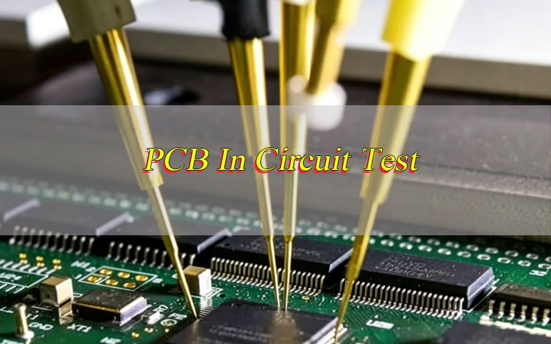
PCB in circuit test is an electrical test that verifies the functionality and integrity of individual components and their connections on a PCB without removing them. Unlike visual inspection, which only catches surface-level issues, in-circuit testing of PCB evaluates the electrical performance of each component to ensure they meet design specifications and proper soldering.
The essential nature of PCB in circuit test stems from its ability to catch hidden defects early in manufacturing. Below are the reasons PCB in circuit test is non-negotiable for PCB assemblies:
- Reduce rework costs dramatically: Fixing a faulty component during assembly costs a fraction of repairing or replacing a finished product, especially in industries like automotive, aerospace, or medical devices.
- Ensure reliability: Reliability is non negotiable in critical industries, and PCB in circuit test verifies components meet design standards to prevent failures.
- Maintain production consistency: It ensures consistency across production runs, minimizing product recall risks and protecting brand reputation.
Without PCB in circuit test, manufacturers risk shipping products with latent defects such as cold solder joints, incorrect component values, or short circuits. These defects lead to product failure, safety risks, and lost customer trust. For high volume production, in circuit testing pcb is necessary to maintain efficiency and quality standards.
What Are the Methods of PCB ICT: Bed of Nails vs. Flying Probe?
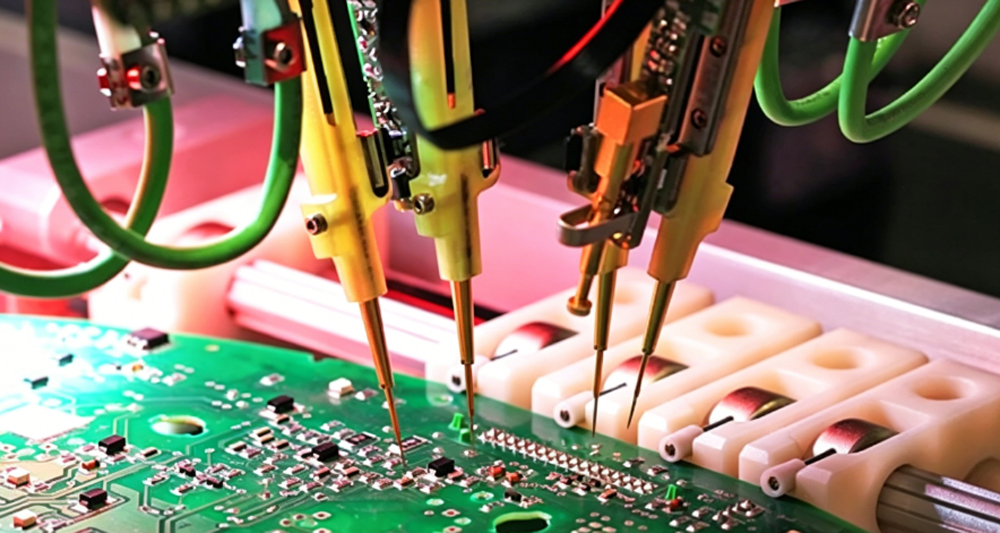
The two primary methods of in-circuit testing PCB are Bed of Nails and Flying Probe. Below is a detailed comparison of the two methods, focusing on factors customers care about most:
| Comparison Factor | Bed of Nails ICT | Flying Probe ICT |
|---|---|---|
| Upfront Cost | Higher (requires custom fixtures, $2,000–$20,000+) | Lower (no custom fixtures needed) |
| Test Speed | Fast (10–60 seconds per board), ideal for high volume | Slow (1–5 minutes per board), not ideal for high volume |
| Accuracy & Repeatability | High (fixed probes ensure consistent contact) | Slightly lower (movable probes may miss test points if uncalibrated) |
| Flexibility | Low (fixtures become obsolete if PCB design changes) | High (no fixtures, suitable for prototypes/design changes) |
| Suitability for High-Density PCBs | Possible (requires custom fixtures with small, closely spaced probes) | Ideal (movable probes access hard-to-reach test points) |
| Best For | High-volume production with stable PCB designs | Low-volume production, prototypes, frequent design changes |
How Does PCB In Circuit Test Work in Step-by-Step Processes?
Describe the process of in circuit test in pcb involves a structured, step-by-step approach that ensures thorough and accurate testing. While the exact steps may vary slightly based on the test method and equipment, the core process remains consistent:
Step 1: Test Preparation
- Create a test program using the PCB’s gerber files and bill of materials (BOM), defining components to test, expected values, and test points.
- For Bed of Nails ICT: Design and manufacture a custom fixture aligned with the PCB’s test points.
- For Flying Probe ICT: Program probe paths into the equipment.
Step 2: PCB Placement
- Place the PCB in the test fixture (Bed of Nails) or on the test platform (Flying Probe).
- Secure the PCB (e.g., vacuum suction) to ensure stable probe contact and prevent movement during testing.
Step 3: Probe Contact
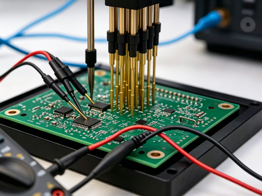
- Bed of Nails: Lower the fixture to bring spring-loaded probes into contact with test points.
- Flying Probe: Movable probes navigate to each test point, making contact sequentially.
- The in circuit tester pcb sends a small electrical signal through each probe to the component being tested.
Step 4: Electrical Testing
- Test equipment measures the component’s electrical response and compares it to expected values in the test program.
- Tests include: short circuits, open circuits, incorrect component values, poor solder joints, diode polarity, transistor functionality, and capacitor capacitance.
Step 5: Defect Identification and Reporting
- Flag defects, identify their PCB location, and record details in a test report (e.g., short circuit between two traces).
- Report simplifies defect resolution by clarifying the issue and affected component.
Step 6: Retesting (If Needed)
- Retest the PCB after defect repair to confirm the issue is resolved and no new defects were introduced.
What Common PCB Assembly Defects Can ICT Detect?
In-circuit testing pcb is highly effective at detecting a wide range of common PCB assembly defects, many of which are invisible to visual inspection. Catching these defects early prevents them from causing more serious issues in finished products. Key defects ICT detects include:
Open Circuits
- Cause: Poor solder joints, broken traces, or missing components.
- Detection: High resistance reading between test points.
Short Circuits
- Cause: Excess solder (solder bridges) or misplaced components.
- Detection: Lower than expected resistance between test points.
Incorrect Component Values
- Cause: Installation of a component with the wrong value (e.g., 1kΩ resistor instead of 10kΩ).
- Detection: Compares measured electrical properties (resistance, capacitance) to BOM expected values.
Missing Components
- Detection: Open circuit or lack of electrical response from the expected component location.
Reverse Polarity
- Affects: Diodes, capacitors, LEDs (components with specific polarity requirements).
- Detection: Incorrect electrical response to test signals.
Cold Solder Joints
- Cause: Insufficient heat during soldering (poor electrical connection).
- Detection: Inconsistent resistance or intermittent connections at the joint.
What Is the Difference Between PCB ICT and Functional Testing (FCT)?
PCB ICT and Functional Testing (FCT) are both critical quality control measures, but they serve different purposes. Below is a clear comparison focusing on customer-critical differences:
| Comparison Factor | PCB in Circuit Test (ICT) | Functional Testing (FCT) |
|---|---|---|
| Test Focus | Individual components and their connections (tests components in isolation) | Overall PCB functionality as a complete system (simulates real-world use) |
| Test Timing | Early in manufacturing (after soldering, before final assembly) | Late in manufacturing (after full PCB assembly) |
| Defects Detected | Component-level defects (open/short circuits, incorrect values, poor solder joints) | System-level defects (failure to perform designed tasks) |
| Example Test | Measure resistor resistance or capacitor capacitance | Test power supply PCB’s ability to convert input voltage |
In summary, ICT catches component level defects, while FCT catches system level defects. Both are necessary for a comprehensive quality control program. ICT ensures the PCB’s components are sound, and FCT ensures the PCB works as intended in real world use.
What Is the Cost of PCB ICT and Which Factors Influence Pricing?
The cost of PCB in circuit test varies widely based on factors that directly impact a manufacturer’s budget. Below are the cost-influencing factors, broken down for clarity:
Test Method
- Bed of Nails ICT: Higher upfront costs (custom fixtures: $2,000–$20,000+), lower per-unit costs.
- Flying Probe ICT: Lower upfront costs (no fixtures), higher per-unit costs (longer test times).
Equipment Costs
- Basic Flying Probe systems: $10,000+.
- High-speed Bed of Nails systems: $100,000+.
- Used equipment: 30–50% cost reduction, but higher maintenance needs.
PCB Complexity
- Complex/high-density PCBs require advanced equipment, longer test programs, and specialized probes/fixtures increasing costs.
Production Volume
- High volume: Bed of Nails is more cost-effective (fixture costs spread over thousands of units).
- Low volume/prototypes: Flying Probe is more cost-effective (avoids expensive fixtures).
Test Program Development
- Cost: $500–$5,000+ (varies by PCB complexity; includes programming, component library setup, test validation).
Maintenance Costs
- 5–10% of initial equipment cost per year (includes probe replacement, fixture repairs, software updates).
What Common ICT Issues Arise in PCB Testing and How to Resolve Them?
PCB in circuit test is reliable, but common issues can lead to inaccurate results, delays, or higher costs. Below are the most frequent issues, along with actionable solutions customers need:
Probe Contact Issues
- Common Causes: Dirty test points, worn probes, misaligned fixtures.
- Solutions: Clean test points with isopropyl alcohol; replace worn probes; calibrate fixtures for proper alignment; use systems with contact impedance monitoring to detect issues early.
Test Program Errors
- Common Causes: Incorrect component values, missing test points in the program.
- Solutions: Validate the test program against gerber files and BOM before production; update the program whenever the PCB design changes.
False Failures
- Common Causes: Temperature fluctuations, component tolerances, incorrect test thresholds.
- Solutions: Adjust test thresholds for component tolerances; control test environment (consistent temperature/humidity); calibrate equipment regularly.
Fixture Wear and Tear
- Common Causes: Regular use leading to worn springs, probes, or fixture damage.
- Solutions: Inspect fixtures regularly for damage; replace worn components; store fixtures in a clean, dry environment when not in use.
Test Time Delays
- Common Causes: Redundant tests, inefficient probe paths (Flying Probe), complex PCBs.
- Solutions: Optimize test programs to remove redundancies; prioritize critical components; use high-speed probes (Bed of Nails); program Flying Probe paths for efficiency.
How to Optimize PCB In Circuit Testing for Higher Efficiency and Testing Accuracy?
Optimizing in circuit testing PCB reduces costs, speeds up production, and improves accuracy. Below are actionable strategies to maximize test effectiveness:
Design for Testability (DFT)
- Add sufficient test points (at least one per component pin) in accessible locations.
- Avoid test point crowding; design clear trace paths to minimize interference.
Optimize Test Programs
- Regularly review and update programs to remove redundant tests and prioritize critical components.
- Use software tools to automate program generation (reduces errors and programming time).
- Use parallel testing for high volume production (test multiple PCBs at once).
Calibrate Equipment Regularly
- Calibrate the in circuit tester pcb every 6–12 months (per manufacturer recommendations).
- Keep detailed calibration records to track equipment performance.
Implement Real Time Monitoring
- Track test results, equipment performance, and defect rates in real time.
- Quickly identify trends (e.g., sudden increase in false failures) and resolve bottlenecks.
Is ICT Applicable to All PCB Assemblies, Especially High-Density PCBs?
PCB in circuit test is applicable to most PCB assemblies, including high density PCBs. Below is a breakdown of applicability, focusing on high-density boards (a key customer concern):
Flying Probe ICT for High-Density PCBs
- Preferred method: Small, movable probes access hard-to-reach test points.
- Advantages: Navigates tight spaces/small components; suitable for complex high-density designs; some systems use high-frequency probes for high-speed components.
Bed of Nails ICT for High-Density PCBs
- Possible but costly: Requires custom fixtures with small, closely spaced probes.
- Advantages: Faster test times for high volume production; requires advanced design software for precise fixture alignment.
Limitations
- ICT is not fully applicable for PCBs with no accessible test points or fully embedded components.
- Solution: Use alternative methods (X ray inspection, boundary scan testing) alongside ICT for comprehensive defect detection.
What Are the Best Practices for PCB ICT Implementation in High-Volume Production?
For high-volume production, efficient and accurate PCB in circuit test implementation is critical. Below are the best practices to ensure scalability and quality:
Choose the Right Test Method
- Prioritize Bed of Nails ICT (fast test times) for high volume; use high-speed systems that test multiple PCBs simultaneously.
- Hybrid approach: Bed of Nails for stable designs, Flying Probe for prototypes/design changes.
Standardize Test Processes
- Standardize test program development, equipment calibration, and defect reporting across production lines.
- Reduces errors and ensures consistency.
Integrate ICT with Other Quality Control Processes
- Pair with Automated Optical Inspection (AOI) to catch surface-level defects before ICT (reduces electrical test workload).
- Use X ray inspection to detect hidden defects (e.g., BGA solder joints) that ICT may miss.
Use Data Analytics to Drive Improvements
- Collect and analyze test data to identify trends, bottlenecks, and frequent defects.
- Investigate root causes of recurring failures (e.g., poor soldering) and implement corrective actions.
Maintain Equipment and Fixtures
- Establish a regular maintenance schedule; replace worn probes/fixture components promptly.
- Clean equipment regularly to prevent dirt/debris from affecting accuracy; reduces downtime.
FAQs About PCB in Circuit Test
Q1: Can PCB in circuit test detect all types of PCB assembly defects?
A1: No, PCB in circuit test cannot detect all defects. It excels at detecting component level defects like open circuits, short circuits, incorrect component values, and poor solder joints. However, it cannot detect defects like cracked traces (unless they cause an open circuit), embedded component defects, or some types of BGA solder joint issues. For these defects, additional testing methods like X ray inspection or boundary scan testing may be needed.
Q2: How long does PCB in circuit test take per board?
A2: Test time varies based on the test method and PCB complexity. Bed of Nails ICT typically takes 10 to 60 seconds per board, making it ideal for high volume production. Flying Probe ICT takes longer, usually 1 to 5 minutes per board, due to the sequential movement of the probes. Complex PCBs with more components will have longer test times regardless of the method.
Q3: Is PCB in circuit test necessary for low volume production?
A3: Yes, PCB in circuit test is still necessary for low volume production, especially for applications where reliability is critical (e.g., medical devices, aerospace components). Flying Probe ICT is more cost effective for low volume, and it still catches defects that visual inspection would miss, reducing rework costs and ensuring product quality. For low volume prototypes, ICT also helps validate the PCB design before full production.
Q4: Can PCB in circuit test damage the PCB or its components?
A4: No, PCB in circuit test is non destructive when performed correctly. The test equipment uses low voltage signals to measure component performance, which does not damage the PCB or its components. However, improper probe contact (e.g., excessive pressure) or incorrect test settings can cause damage, which is why regular calibration and proper training are essential.
Q5: How often should test programs be updated for PCB in circuit test?
A5: Test programs should be updated whenever the PCB design changes (e.g., new components, changed test points, modified trace paths). They should also be reviewed regularly (every 3 to 6 months) to optimize test efficiency, remove redundant tests, and ensure compatibility with new component libraries. If defect rates increase, the test program should be audited to identify and fix any errors.
Q6: What is the difference between in-circuit testing pcb and in-circuit testing of pcb?
A6: There is no functional difference between in-circuit testing pcb and in-circuit testing of pcb. Both terms refer to the same electrical test method that verifies component functionality and connections on a printed circuit board. The difference is simply in phrasing; both are commonly used in the industry and refer to the same process.
Q7: Can PCB in circuit test be automated for high volume production?
A7: Yes, PCB in circuit test can be fully automated for high volume production. Automated Bed of Nails systems can be integrated into production lines, with robotic arms feeding PCBs into the test fixture and removing them after testing. Test results are automatically recorded and analyzed, and defective boards are routed to a rework station. Automation reduces human error, increases throughput, and ensures consistent test results.