 language
Tombstoning PCB: Causes, Effects, and Prevention in SMT Assembly
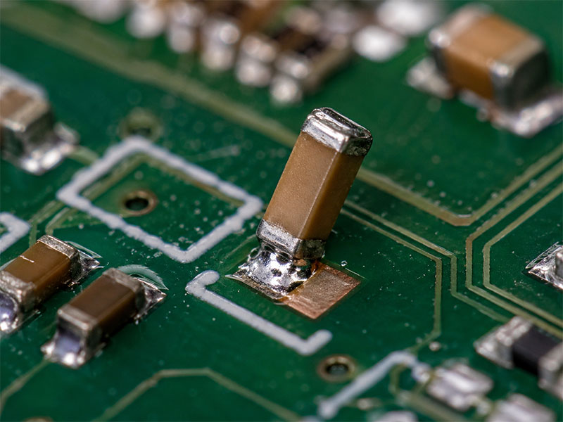
Tombstoning PCB, also known as Manhattan effect or drawbridging, is a critical surface-mount technology (SMT) defect where a small, two-terminal component like a resistor or capacitor lifts vertically on one end during reflow soldering, resembling a tombstone. This article provides a comprehensive analysis of the tombstone effect in PCB assembly, covering its root causes, the underlying physics, and proven prevention strategies to enhance manufacturing yield.
In SMT assembly, achieving perfect solder joints for miniature components is challenging. PCB tombstoning is a persistent headache that can derail production lines and impact product reliability. What are the common frustrations you face?
- Frequent rework due to mysterious component lift-off on the assembly line.
- Inconsistent yields with small chip components like 0603 or 0402 sizes.
- Debugging nightmares where the defect source is unclear—is it the solder paste, the machine, or the design?
- Cost overruns from wasted components, board scrap, and extended troubleshooting time.
- Quality risks as latent tombstone defects may pass inspection only to fail in the field.
Addressing tombstone defect in PCB requires a systematic approach from design to process. As a professional PCBA manufacturer, Best Technology implements robust process controls and design-for-manufacturability (DFM) checks to mitigate these issues.
- Implementing optimized stencil designs to control solder volume and deposition accurately.
- Fine-tuning placement machine calibration and maintenance schedules to ensure perfect component alignment.
- Establishing a rigorous process audit system to isolate variables from paste printing to reflow.
- Applying cost-control through prevention, reducing scrap and rework by identifying root causes early.
- Enforcing strict quality gates with automated optical inspection (AOI) to catch defects before they escalate.
At Best Technology, we specialize in high-quality, reliable PCB assembly. With deep expertise in SMT process optimization and a commitment to excellence, we help our clients navigate complex manufacturing challenges like tombstoning in PCB. Our engineering team works proactively to prevent defects, ensuring your products are built to the highest standards. For inquiries, pls feel free to contact us at sales@bestpcb.vn.

What Is Tombstoning In PCB?
Tombstoning in PCB assembly is a soldering defect specific to Surface Mount Technology (SMT). It occurs when a small, passive chip component (e.g., resistor, capacitor) with two terminations stands up on one of its ends during the reflow soldering process. Instead of lying flat on the board, the component forms a vertical bridge, which visually resembles a tombstone—hence the name. This defect, also called the Manhattan effect or drawbridging, results in an open circuit, rendering the assembly non-functional. The phenomenon is primarily driven by an imbalance in the wetting forces acting on the component’s two terminals.
Key Characteristics of PCB Tombstoning:
- Components Affected: Primarily lightweight, two-terminal chip components (e.g., 01005, 0201, 0402, 0603 packages).
- Visual Result: One end of the component is soldered correctly, while the other end is lifted off its pad.
- Primary Cause: A significant imbalance in the molten solder’s surface tension (wetting force) between the two component terminals.
- Outcome: An electrical open failure.
Table: Common Terms for Tombstoning
| Term | Description |
|---|---|
| Tombstoning | The most common term, describing the component’s vertical stance. |
| Manhattan Effect | Another widely used term, drawing an analogy to city skylines. |
| Drawbridging | Describes the component lifted at an angle, like a drawbridge. |
| Stonehenge Effect | A less common term, also referring to the vertical standing. |
In summary, tombstoning is a critical process failure mode in SMT that must be prevented through careful control of design and process parameters to ensure assembly yield and reliability.
What Is the Torque Principle Behind PCB Tombstoning?
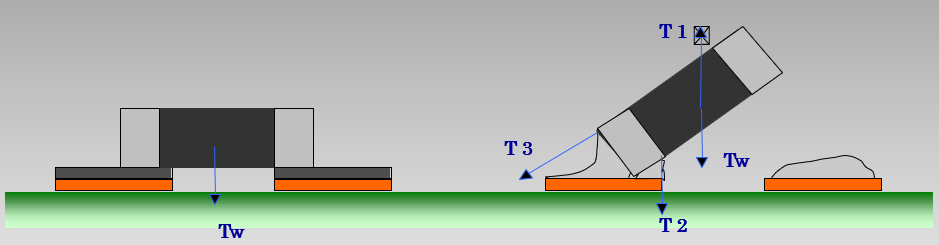
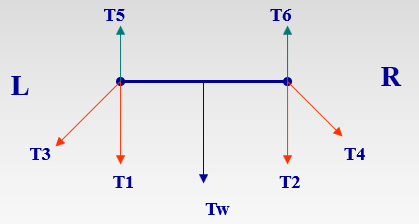
The tombstone effect in PCB is fundamentally a problem of rotational torque. When the solder paste melts during reflow, it creates upward forces on the component terminals. An imbalance in these forces generates a torque that can rotate the component. The principle can be understood by analyzing the key forces and moments involved.
Forces and Torques During Reflow:
- T3 & T4 (Solder Pulling Forces): The primary forces are the vertical surface tension forces (T3 and T4) acting at the top edges of the molten solder fillets on each component terminal. These are the “wetting forces” that pull the component terminal into the solder.
- Tw (Component Weight): The downward force due to the component’s mass, which is typically very small for chip components.
- T1 (Solder Buoyancy): The upward buoyant force exerted by the molten solder.
- Resultant Torque: The tombstone occurs when the combined rotational effect (torque) from T3 and T4 is unequal. The component rotates towards the side with the later-melting, weaker, or absentsolder fillet.
Causes of Torque Imbalance Leading to PCB Tombstoning:
- Asymmetric Solder Volume: Different amounts of solder paste on the two pads (e.g., from uneven stencil printing or paste slump) create unequal T3/T4 forces.
- Non-Simultaneous Melting: One solder joint melts and starts wetting significantly earlier than the other. The earlier-melting side exerts a pulling force (T3/T4) before the opposite side can counterbalance it.
- Component Placement Offset: If the part is misaligned, one terminal may have more contact with the molten solder, leading to a stronger wetting force on that side.
- Asymmetric Pad Thermal Mass: If one pad is connected to a large copper plane (like a ground pour), it heats up more slowly, causing delayed solder melting on that side and creating a timing imbalance in T3/T4.
The Governing Principle: Tombstoning happens when the net torque from the wetting forces overcomes the component’s stability. The condition is often summarized as: T3 ≠ T4. When T3 and T4 are equal and opposite, the component settles correctly. When they are unbalanced, rotation occurs.
In conclusion, understanding the torque principle behind PCB tombstoning is essential for diagnosing and solving the problem, as all prevention strategies aim to balance these critical forces.
How Does the Tombstone Effect in PCB Occur During Reflow Soldering?
The tombstone effect in PCB manifests specifically during the reflow soldering stage. The process involves heating the assembly to melt the solder paste. The defect occurs due to dynamic and uneven wetting behavior as the paste transitions from solid to liquid. The sequence of events typically follows a critical failure path.
Typical Sequence of Tombstone Formation During Reflow:
- Preheat & Soak: The board heats up. Differences in pad size, thermal mass, or paste composition can cause one pad’s solder paste to become active (flux activating, powder coalescing) slightly before the other.
- Liquidus & Wetting Initiation: As the temperature passes the solder’s melting point, the paste turns liquid. If one joint melts and begins to wet its component terminal even a fraction of a second earlier, it starts to exert an upward pulling force (T3 or T4).
- Torque Application: This unilateral upward force on one end of the component creates a rotational torque. The component, being very lightweight, begins to pivot on the edge of the still-solid or just-starting-to-melt solder paste on the opposite pad.
- Liftoff and Finalization: The pivoting action lifts the terminal on the slower-wetting side away from its pad. By the time the solder on that pad finally melts, the terminal is no longer in contact, preventing joint formation. The component remains permanently vertical, soldered only on one side.
Key Factors During Reflow that Trigger Tombstoning:
- Excessively High Preheat Rate: Can cause violent flux activation and uneven paste behavior.
- Insufficient Soak/Preheat Time: Fails to equalize temperature across the board, leading to large thermal gradients and non-simultaneous melting.
- Peak Temperature Too High: Increases the wetting force strength and speed, amplifying any small initial imbalance. It can also lead to excessive wicking.
- Asymmetric Heating: Caused by PCB layout, where one pad is on a thick trace or ground plane (acting as a heat sink) and the other is on a small, isolated trace.
Table: Reflow Profile Parameters and Tombstone Risk
| Reflow Parameter | Incorrect Setting (High Risk) | Corrective Action (Prevention) |
|---|---|---|
| Preheat Rate | Too steep | Use a gentler, controlled ramp. |
| Soak Time | Too short | Extend to ensure board temperature uniformity. |
| Peak Temperature | Too high | Reduce to the minimum required for good wetting. |
| Time Above Liquidus (TAL) | Excessive | Optimize to sufficient but not excessive duration. |
| Cooling Rate | Too steep after liquidus | Use a controlled cooling ramp. |
Ultimately, the tombstone defect in PCB during reflow is a race condition in wetting. Any process or design factor that creates a difference in the timingor magnitudeof the wetting forces between the two component terminals can initiate the defect.
How to Prevent Tombstoning in PCB Assembly?
Preventing tombstoning in PCB assembly requires a holistic approach that addresses design, materials, and process. The goal is to eliminate the conditions that create an imbalance in wetting forces. Successful prevention turns reactive debugging into proactive process control.
Core Strategies for Tombstoning Prevention:
- Optimize Stencil Design and Solder Paste Printing:
- Reduce Outer Pad Solder Volume: For rectangular pads, consider reducing the stencil aperture size on the outer end of the pad. This reduces the solder volume (T3 force) that can pull the component sideways.
- Use Modified Aperture Shapes: Implement home-plate, dog-bone, or other modified stencil aperture designs. These shapes can alter the melt sequence, creating a deliberate and controlled wetting sequence that counteracts lifting forces.
- Ensure Print Consistency: Maintain proper stencil gasketting, squeegee pressure, and cleaning to achieve uniform, aligned solder paste deposits on both pads.
- Fine-Tune Reflow Soldering Profile:
- Ensure Adequate Soak Time: A sufficient preheat/soak stage allows the entire PCB assembly to reach a uniform temperature before the solder melts, minimizing thermal gradients.
- Control Peak Temperature and Ramp Rates: Avoid excessively high peak temperatures and steep temperature ramps into the liquidus phase, which can cause violent and uneven wetting.
- Optimize for Your Solder Paste: Follow the solder paste manufacturer’s recommended profile, as the flux chemistry directly impacts wetting time and force.
- Ensure Precise Component Placement:
- Minimize Placement Offset: Calibrate pick-and-place machines regularly to ensure components are centered accurately on their pads. Even minor misalignment can be a primary cause of PCB pick and place tombstone phenomena.
- Maintain Equipment: Implement regular preventive maintenance for feeders, nozzles, and vision systems to sustain placement accuracy.
- Optimize PCB Pad Layout and Design:
- Avoid Oversized Pads: Follow IPC land pattern standards. Pads that are excessively long, particularly outward from the component, increase the lever arm for the solder’s pulling force (T3), making tombstoning more likely. A guideline suggests the pad extension beyond the component should be less than half the component thickness (L < t/2).
- Balance Thermal Mass: Design symmetrical thermal relief for pads, especially if one pad is connected to a large copper pour. This helps both sides reach soldering temperature simultaneously.
- Consider Material and Atmosphere:
- Solder Paste Selection: While highly active solder pastes wet quickly, they can increase the risk by magnifying small imbalances. For error-prone designs, a paste with a slightly longer wetting time may be beneficial.
- Nitrogen (N2) Reflow: Using a nitrogen atmosphere reduces oxidation, leading to faster, stronger wetting. This can actually increase tombstone effect in PCB risk if other imbalances exist, as the process window becomes narrower. It requires excellent process control.
By systematically implementing these measures, manufacturers can effectively control the variables that lead to PCB tombstoning and achieve high first-pass yields.
What Other Factors Can Cause Tombstone Defects in PCB?
Beyond the primary process factors, several other design and material considerations can significantly contribute to tombstone defects in PCB. These factors often interact with the reflow process to create the precise conditions for force imbalance.
Additional Contributing Factors to Tombstoning:
- PCB Pad Design Issues:
- Asymmetric Pad Size/Shape: Differently sized or shaped pads for the same component will have different solder volumes and thermal characteristics, directly causing wetting imbalance.
- Pad with Uneven Thermal Connection: A classic case is when one pad is connected directly to a large ground plane (acting as a heat sink) while the other is connected to a thin signal trace. This creates a large temperature difference during reflow, a major cause of PCB layout tombstone issues.
- Solder Paste Characteristics:
- High Activity Flux: While good for wetting, an overly aggressive flux can lead to excessively rapid and strong wetting forces, leaving no time for the opposing joint to catch up.
- Slumping: Solder paste with poor anti-slump properties can spread or bridge before reflow, altering the intended solder volume distribution on the pads.
- Alloy Composition: Some studies, as noted in the provided documents, indicate that adding a small percentage of silver (Ag) to SnPb solder can modify the solidification behavior, spreading the eutectic action over a temperature range and reducing the instantaneous pulling force, thereby lowering Manhattan defect rates.
- Component-Related Factors:
- Extremely Light Weight: Smaller packages (e.g., 0201, 01005) have minimal mass (Tw), offering less resistance to rotational torque from wetting forces.
- Termination Finish: The wettability of the component’s end terminations must be consistent. Poor or non-uniform plating can cause one end to wet poorly or slowly.
- Use of Nitrogen (N2) Atmosphere in Reflow:
- This is a double-edged sword. While N2 reduces oxidation and improves joint quality, it also results in faster, more uniform wetting. This effectively “amplifies” any existing small imbalance in solder volume, placement, or thermal design. Therefore, tombstoning in PCB assembly can sometimes become more prevalent in a nitrogen environment unless the upstream process is very well controlled.
- Secondary Reflow or Rework:
- Boards undergoing a second reflow cycle or localized rework may experience tombstoning on previously good joints. This can be due to additional oxidation, flux depletion, or thermal stress altering the solder joint geometry.
Understanding these ancillary factors is crucial for comprehensive root cause analysis when tackling persistent tombstone PCB issues, especially when standard process corrections do not yield results.
What Are the Main Types of SMT Tombstoning in PCB Assembly?
While the final physical manifestation is similar, SMT tombstoning in PCB assembly can be categorized based on the severity and orientation of the lift. The type can sometimes give clues about the primary cause. The fundamental classification revolves around the degree of rotation and the point of pivot.
Classification of Tombstone Defects:
Complete Tombstoning (Vertical Lift):
- Description: The component is standing completely vertical, with one terminal fully soldered and the other completely lifted off its pad. This is the classic “tombstone” or “Manhattan” appearance.
- Likely Cause: A severe initial imbalance, such as a complete lack of solder on one pad, a significant placement offset, or a large thermal mass difference causing one joint to melt much later than the other.
Partial Tombstoning (Angular Lift or Drawbridging):
- Description: The component is lifted at an angle but is still making some contact with the pad on the “lifted” end. The solder fillet on the lifted side may be very thin or only on the heel of the termination.
- Likely Cause: A less severe but still significant imbalance. This could result from a slight solder volume difference, a minor placement error, or a small thermal gradient. The component started to rotate but the opposite joint wetted just in time to partially arrest the motion.
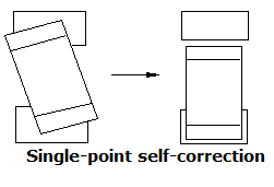
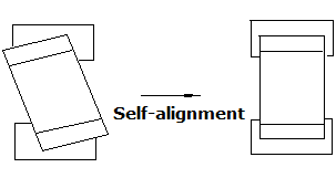
Self-Alignment (Intentional Correction):
- Description: This is the desired outcome, not a defect. If a component is placed with a slight offset but the pad design, solder volume, and reflow profile are optimal, the surface tension from bothsimultaneously melting solder joints can pull the component into perfect alignment. This highlights the power of balanced forces.
- Key Condition: It requires near-simultaneous melting and sufficient, symmetrical wetting forces on both sides.
Increased Misalignment (Failed Self-Alignment):
- Description: The opposite of self-alignment. A minor initial placement offset is made worse during reflow. The wetting force on the side with better contact becomes dominant and pulls the component further toward that side, potentially leading to a skewed joint or even a partial tombstone.
- Likely Cause: Conditions that prevent the opposing wetting force from developing properly, such as poor solderability on one pad or a significant solder volume difference.
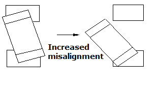
Table: Tombstone Types and Probable Root Causes
| Type | Visual Description | Probable Primary Cause Area |
|---|---|---|
| Complete Tombstone | Component vertical, one end fully off pad. | Severe solder volume deficit, major placement error, large thermal asymmetry. |
| Partial Tombstone / Drawbridge | Component at an angle, one end partially connected. | Moderate solder volume difference, slight placement offset, minor thermal imbalance. |
| Increased Misalignment | Component skewed from its placed position, both ends connected. | Asymmetric wetting strength failing to correct initial minor offset. |
Recognizing these types helps diagnosticians narrow down the potential root causes, making the troubleshooting process for what is tombstoning in PCB issues more efficient.
In conclusion, tombstoning PCB is a complex defect rooted in the physics of wetting forces and torque imbalance during reflow soldering. This article has detailed its causes—from pad design and thermal asymmetry to paste printing and reflow profiles—and outlined effective prevention strategies focused on balancing these forces.
Successfully preventing the tombstone effect in PCB assembly requires expertise, precise process control, and attention to detail at every stage, from DFM review to final inspection. At Best Technology, we leverage our deep SMT process knowledge and rigorous quality systems to help our clients eliminate defects like tombstoning and achieve exceptional manufacturing yields. Pls feel free to contact us anytime at sales@bestpcb.vn to discuss your requirements.
FAQs About Tombstoning PCB
Can PCB layout cause tombstoning?
Yes, PCB layout is a major contributor to tombstoning. The most common issue is asymmetric thermal mass. For example, if one pad of a resistor is connected to a large ground plane (a heat sink) and the other to a thin trace, the grounded side will heat up much more slowly during reflow. This causes the solder on that pad to melt later, creating the critical timing imbalance that leads to the component being pulled toward the hotter side. Pad size and symmetry are also part of PCB layout tombstone considerations.
How can pad design prevent PCB tombstoning?
Optimal pad design is a primary preventive measure. Key principles include:
- Symmetry: Pads must be identical in size, shape, and thermal connection.
- Appropriate Size: Avoid overly long pads, especially outward from the component. A guideline suggests the pad extension beyond the component body should be less than half the component’s thickness to reduce the lever arm for the lifting force.
- Thermal Relief: Use thermal relief connections for pads attached to copper pours to balance heating.
Is tombstoning a soldering defect or a PCB design issue?
Tombstoning is typically a process defect, but it is often triggered or exacerbated by a marginal PCB design. A perfect reflow process can sometimes overcome a poor design, and a perfect design can tolerate minor process variations. However, tombstoning most frequently occurs at the intersection of a susceptible design (e.g., asymmetric pads) and a process that is not optimized to compensate for it (e.g., an aggressive reflow profile). Therefore, it requires evaluation of both areas.
How does reflow temperature affect tombstoning?
The reflow temperature profile is critical. An excessively high peak temperature or too rapid a ramp-up increases the wetting force and speed, amplifying any small initial imbalance. Conversely, insufficient or uneven heating (soak) can cause non-simultaneous melting. An optimized profile with a proper soak for temperature stabilization and a controlled peak temperature is essential to minimize tombstoning in PCB.
Can pick and place offset cause tombstoning?
Absolutely. Pick and place offset is a direct and common cause. If the part is not centered, one termination will have more overlap with its solder paste deposit than the other. During reflow, the side with better contact will wet earlier and more strongly, pulling the component and causing PCB pick and place tombstone phenomena. Regular machine calibration and maintenance are vital to prevent this.