 language
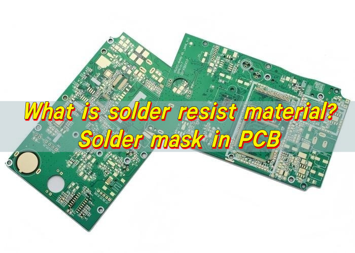
What is Solder Resist Material? Solder Mask in PCB
What is solder resist?
Solder resist material, often referred to as solder mask in PCB manufacturing, is a polymer-based protective coating applied to the surface of a printed circuit board. Its primary function is to prevent unwanted solder bridging during assembly, while also shielding copper traces from oxidation, moisture, and environmental contamination. In practical manufacturing environments, this layer is as critical as the copper circuitry itself because it directly influences yield, reliability, and long-term field performance.
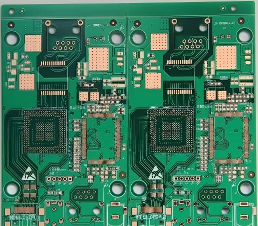
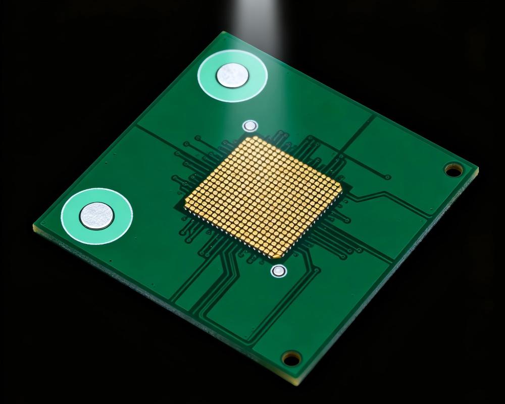
From an engineering standpoint, solder resist serves multiple roles simultaneously. It defines solderable regions with high precision, improves electrical insulation between adjacent conductors, and enhances the visual clarity of the board for inspection. The familiar green color seen on most PCBs is simply a standard pigment choice; the actual function lies in the material chemistry and curing process rather than the color itself.
In modern electronics manufacturing, PCB solder resist material is tightly integrated into design rules. Engineers specify solder mask openings, clearance tolerances, and alignment margins to ensure compatibility with fine-pitch components such as BGAs and QFNs. Without a well-controlled solder resist layer, assembly defects such as solder bridging, insufficient wetting, or contamination-related failures become significantly more likely.
Another subtle yet important benefit is mechanical protection. The coating acts as a barrier against scratches and minor handling damage during assembly and testing. This becomes particularly valuable in high-mix, low-volume production where boards pass through multiple manual handling steps.
For manufacturers like Best Technology, solder mask is not treated as a simple coating step. It is part of a controlled process that directly impacts yield, especially when dealing with HDI boards, fine line spacing, or high-reliability sectors such as automotive and medical electronics.
What is solder resist made of?
Solder resist material is typically composed of epoxy-based or acrylic-based polymers that are engineered to withstand thermal stress, chemical exposure, and electrical demands. These materials are formulated with photoinitiators, pigments, fillers, and curing agents to achieve specific performance characteristics.
At a material level, PCB solder mask material includes:
- Base resin (Epoxy or acrylic)
Provides structural integrity and adhesion to the PCB substrate. - Photoinitiators
Enable UV curing in photoimageable solder mask processes. - Pigments
Define the color (green, black, white, red, blue), though color can also influence optical inspection performance. - Fillers
Enhance mechanical strength and thermal resistance. - Additives
Improve properties such as flame retardancy, flexibility, and chemical resistance.
The most widely used type today is Liquid Photoimageable (LPI) solder mask, which offers excellent resolution and consistency. This material allows precise definition of solder mask openings, making it suitable for fine-pitch components and high-density designs.
From a property perspective, solder resist material property requirements are quite demanding. The material must demonstrate:
- High dielectric strength
- Strong adhesion to copper and laminate
- Resistance to flux, solvents, and cleaning agents
- Thermal stability during reflow (typically 230–260°C)
- Low moisture absorption
For advanced applications, such as RF boards or high-frequency circuits, the dielectric properties of the solder mask can even influence signal integrity. In such cases, material selection becomes more critical and may require specialized formulations.
At Best Technology, material selection is aligned with application requirements. For example, high-Tg solder mask formulations are used for automotive and industrial boards where repeated thermal cycling is expected.
How is solder resist applied?
The solder mask application process is a carefully controlled sequence that directly affects alignment accuracy and final board quality. While several methods exist, the dominant approach in modern PCB fabrication is the photoimageable process.
The typical solder mask application workflow includes:
- Surface preparation
The PCB surface is cleaned and roughened to improve adhesion. - Coating
Liquid solder mask ink is applied using screen printing, curtain coating, or spray coating. - Pre-drying (tack drying)
The coated board is partially dried to remove solvents. - Exposure
UV light is used to define solder mask openings through a photomask. - Development
Unexposed areas are washed away, revealing pads and vias. - Final curing
Thermal curing completes polymer cross-linking, ensuring durability.
This process ensures that solder mask openings align precisely with pads, which is essential for component placement accuracy. Any misalignment can lead to assembly defects, particularly in fine-pitch designs.
In high-volume manufacturing, automated optical inspection (AOI) is often used after solder mask application to verify alignment and detect defects such as pinholes, insufficient coverage, or contamination.
At Best Technology, solder mask application is integrated into a digitalized workflow with tight process control. This ensures consistent thickness, accurate registration, and minimal variation across production batches.
What is the thickness of solder resist?
The thickness of solder resist is a critical parameter that influences insulation performance, mechanical protection, and manufacturability. Typically, solder mask thickness ranges between 10 µm and 30 µm, depending on the application and process method.
A general breakdown is as follows:
| Application Type | Typical Thickness | Key Consideration |
|---|---|---|
| Standard PCB | 15–25 µm | Balanced protection and resolution |
| HDI PCB | 10–20 µm | Fine feature definition |
| Power electronics | 20–30 µm | Enhanced insulation and durability |
Thickness control is essential because excessive thickness can lead to poor pad definition, while insufficient thickness may compromise insulation and protection. Engineers often specify solder mask clearance and expansion values to ensure compatibility with component footprints.
In high-reliability applications, uniform thickness is just as important as nominal thickness. Variations can lead to uneven solder wetting or localized stress during thermal cycling.
Best Technology employs controlled coating and curing processes to maintain tight thickness tolerances, ensuring consistent electrical and mechanical performance across all boards.
What are the four types of solders?
Although this section refers to solder rather than solder resist, understanding solder types helps clarify how solder mask interacts with assembly materials.
The four commonly used solder types include:
- Lead-based solder (Sn-Pb)
Known for excellent wetting and reliability, though increasingly restricted due to environmental regulations. - Lead-free solder (SAC alloys)
Typically composed of tin, silver, and copper. Widely used in compliance with RoHS requirements. - Low-temperature solder
Designed for heat-sensitive components, reducing thermal stress during assembly. - High-temperature solder
Used in applications requiring multiple reflow cycles or extreme operating conditions.
Each solder type interacts differently with solder resist material. For instance, higher reflow temperatures in lead-free processes demand stronger thermal resistance from the solder mask. This is why modern PCB solder mask material is engineered to withstand higher peak temperatures compared to older formulations.
How to choose solder resist?
Selecting the right solder resist material involves balancing electrical, mechanical, and manufacturing requirements. The choice is rarely arbitrary; it is guided by application-specific constraints.
Key factors to consider include:
- Thermal performance
High-Tg materials are preferred for automotive, aerospace, and power electronics. - Resolution capability
Fine-pitch designs require high-resolution LPI solder mask. - Chemical resistance
Important for boards exposed to harsh environments or aggressive cleaning processes. - Color requirements
White masks for LED applications, black for optical systems, green for general use. - Compliance standards
UL, RoHS, REACH, and industry-specific certifications.
For example, LED lighting boards often use white solder mask to improve light reflectivity, while RF boards may require low-loss materials to minimize signal interference.
Best Technology supports material selection through DFM analysis. By evaluating layout, assembly requirements, and end-use conditions, the engineering team ensures that the chosen solder resist type aligns with both performance and manufacturability goals.
Is solder resist the same as solder mask?
In practice, solder resist and solder mask refer to the same concept. The difference lies mainly in terminology rather than function.
- Solder mask is the more commonly used term in PCB manufacturing.
- Solder resist emphasizes the material’s function—resisting solder adhesion in undesired areas.
To clarify the distinction:
| Term | Meaning | Usage Context |
|---|---|---|
| Solder mask | Protective PCB coating | Manufacturing and design |
| Solder resist | Functional description | Material and process discussions |
While the two terms are interchangeable, “solder mask” is more prevalent in documentation, datasheets, and industry communication.
Why does solder iron need thermal resistive material?
A soldering iron requires thermal resistive material primarily to control heat flow and protect both the tool and the operator. While this may seem unrelated to PCB solder resist material, the underlying principle is similar—managing heat effectively.
Thermal resistive materials in soldering irons serve to:
- Maintain stable tip temperature
- Prevent heat loss to surrounding components
- Protect internal electrical elements
- Improve energy efficiency
In PCB assembly, thermal management is equally important. Solder resist material contributes by insulating sensitive areas and preventing unintended heat transfer during soldering or reflow processes.
For high-density boards, controlling thermal distribution is critical to avoid defects such as tombstoning or uneven solder joints. This is why both tooling and PCB materials must work together to achieve consistent results.
How to remove solder resist?
Removing solder resist is sometimes necessary for rework, repair, or modification. However, it must be done carefully to avoid damaging underlying copper traces.
Common methods include:
- Mechanical removal
Using scraping tools or micro-abrasion. Suitable for small areas but requires precision. - Chemical stripping
Specialized solvents can dissolve solder mask without harming copper. - Laser removal
High-precision method used in advanced manufacturing environments.
Each method has its own trade-offs in terms of speed, precision, and risk. For example, mechanical removal is straightforward but may introduce scratches, while chemical methods require controlled handling of solvents.
In professional PCB manufacturing, removal is typically avoided unless absolutely necessary. Instead, design corrections are implemented at the fabrication stage to minimize rework.
Best Technology emphasizes first-pass yield optimization through DFM checks and process control, reducing the need for post-production modifications.
Conclusion:
Solder resist material plays a foundational role in PCB manufacturing. It is far more than a protective coating—it is a functional layer that ensures assembly accuracy, electrical insulation, and long-term reliability. From material composition to application methods and thickness control, every aspect of solder mask influences final product performance.
In modern electronics, where miniaturization and reliability are both critical, solder resist continues to evolve. Advanced formulations and precise application techniques are enabling higher density designs and more demanding applications.
If you are looking for reliable PCB manufacturing and assembly solutions, including optimized solder mask processes, feel free to reach out. For more information or project support, visit: sales@bestpcb.vn