 language
Double Layer PCB Manufacturing Services | Custom & Mass Production
What is double layer PCB manufacturing?
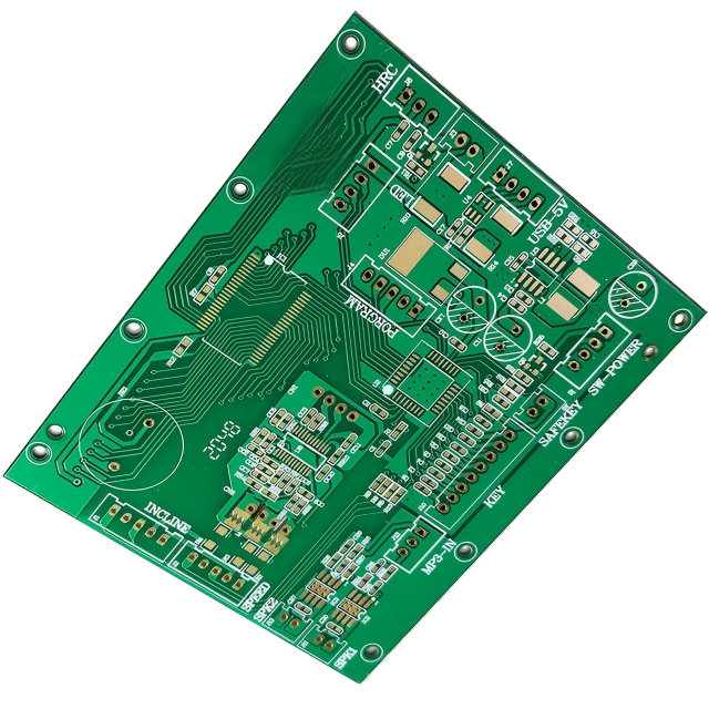
Double layer PCB manufacturing refers to the fabrication of printed circuit boards that contain conductive copper layers on both the top and bottom sides of a substrate, typically connected through plated through holes to enable signal and power transmission across layers. This structure offers a balanced combination of routing flexibility and cost efficiency, which is why it remains one of the most widely used PCB types in both consumer and industrial electronics.
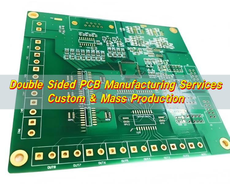
In practical applications, double layer PCB manufacturing allows engineers to design more compact and functional circuits compared to single-sided boards, while still maintaining a relatively simple production process. It is often selected for designs where signal routing becomes slightly complex but does not yet require the density or stackup sophistication of multilayer boards.
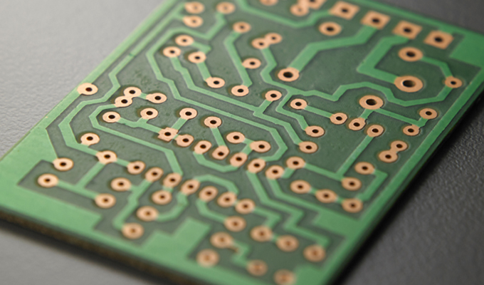
From a manufacturing perspective, the process involves laminating copper onto both sides of a dielectric material, followed by imaging, etching, drilling, and plating steps to form the final circuit pattern. The inclusion of vias enables interconnection between the two layers, which is a defining feature of this type of board.
In engineering terms, double layer PCBs provide a practical middle ground. They support moderate component density, allow better ground referencing, and enable improved signal integrity compared to single-layer designs. For many engineers, this makes them a preferred starting point for cost-sensitive yet performance-conscious projects.
At Best Technology, double layer PCB manufacturing is treated not as a basic service, but as an engineered solution. Every project undergoes DFM analysis to ensure that layout decisions align with production realities, which helps reduce iteration cycles and improve yield consistency.
What steps are involved in double layer PCB manufacturing?
The double sided PCB manufacturing process consists of a series of tightly controlled steps, each contributing to the final electrical performance and mechanical reliability of the board. While the workflow may vary slightly depending on complexity and volume, the core sequence remains consistent across most production environments.
The typical process includes:
- Material preparation: Copper-clad laminate is selected based on design requirements such as Tg, thickness, and dielectric constant
- Inner surface cleaning: Ensures optimal adhesion before pattern formation
- Photo imaging: Circuit patterns are transferred onto both sides using photoresist and UV exposure
- Etching: Unwanted copper is removed to form the desired traces
- Drilling: Mechanical or laser drilling creates holes for vias and component leads
- PTH (Plated Through Hole): Holes are metallized to establish electrical connections between layers
- Solder mask application: Protects copper traces and prevents solder bridging
- Surface finish: Applied to exposed pads to improve solderability and durability
- Electrical testing: Ensures continuity and isolation meet design specifications
- Final inspection and packaging: Boards are verified and prepared for shipment
Each step must be executed with precision, especially drilling and plating, as these directly impact connectivity and long-term reliability.
At Best Technology, process control is enhanced through MES integration, which allows real-time tracking of each panel throughout production. This level of traceability ensures that every board can be linked back to its process parameters, materials, and inspection data.
What materials are used in double layer PCB manufacturing?
Material selection in double layer PCB manufacturing plays a critical role in determining electrical performance, thermal behavior, and long-term stability. While FR4 remains the most common substrate, engineers often choose materials based on specific application requirements.
Common materials include:
- FR4 epoxy laminate: The industry standard for general-purpose applications due to its cost-effectiveness and mechanical strength
- High-Tg FR4: Suitable for environments with elevated operating temperatures
- Rogers materials: Used in RF and high-frequency designs where dielectric stability is essential
- Metal core substrates: Applied in thermal-critical applications such as LED lighting and power electronics
- Polyimide: Selected for flexible or high-temperature environments
The copper layer is equally important. Standard copper thickness ranges from 1 oz to 3 oz, although heavier copper may be used for power applications requiring higher current carrying capacity.
Below is a simplified comparison of common materials:
| Material Type | Key Advantage | Typical Application | Cost Level |
|---|---|---|---|
| FR4 | Balanced performance | Consumer electronics | Low |
| High-Tg FR4 | Better thermal stability | Industrial control | Medium |
| Rogers | Low signal loss | RF communication | High |
| Metal Core | Excellent heat dissipation | LED, power modules | Medium–High |
Best Technology supports a wide range of material options and provides engineering guidance during the selection phase. This ensures that the chosen substrate aligns with both performance targets and cost expectations.
Why is PTH important in double layer PCB manufacturing?
Plated Through Hole technology is fundamental to double layer PCB manufacturing because it enables electrical connectivity between the top and bottom copper layers. Without PTH, the two sides of the board would function independently, which would severely limit design flexibility.
The importance of PTH can be understood from several perspectives. First, it allows signals to transition between layers, making complex routing possible even within a relatively simple two-layer structure. Second, it provides mechanical support for through-hole components, improving structural integrity during assembly and operation.
From a reliability standpoint, the quality of the plating inside the hole is critical. Poor plating can lead to issues such as open circuits, intermittent connections, or long-term fatigue failures due to thermal cycling.
Key benefits of PTH include:
- Reliable electrical interconnection between layers
- Enhanced mechanical strength for component mounting
- Improved current carrying capability in vertical paths
- Compatibility with both through-hole and mixed-technology assemblies
At Best Technology, PTH quality is controlled through strict process parameters, including plating thickness, hole wall roughness, and chemical composition. Advanced inspection methods such as microsection analysis are used to verify plating integrity.
What surface finishes are available for double layer PCBs?
Surface finish is applied to exposed copper pads to protect them from oxidation and to ensure reliable soldering during assembly. The choice of surface finish affects not only manufacturability but also long-term performance and shelf life.
Common surface finishes include:
- HASL (Hot Air Solder Leveling): A cost-effective option suitable for general applications
- ENIG (Electroless Nickel Immersion Gold): Offers excellent flatness and corrosion resistance
- OSP (Organic Solderability Preservative): A simple and environmentally friendly solution
- Immersion Silver: Provides good conductivity and solderability
- ENEPIG: Used for high-reliability and wire bonding applications
Each finish has its own characteristics, and the selection depends on factors such as component pitch, assembly method, and environmental exposure.
A comparison is shown below:
| Surface Finish | Flatness | Shelf Life | Application Suitability |
|---|---|---|---|
| HASL | Moderate | Medium | General electronics |
| ENIG | Excellent | Long | Fine-pitch components |
| OSP | Good | Short | Cost-sensitive designs |
| Immersion Silver | Good | Medium | RF and high-speed circuits |
Best Technology helps customers select the most suitable finish based on assembly requirements and product lifecycle expectations, ensuring both performance and manufacturability.
What testing is done in double layer PCB manufacturing?
Testing is a critical phase in double layer PCB manufacturing, as it verifies that the fabricated board meets electrical and structural specifications before it proceeds to assembly or shipment.
The most common testing methods include:
- Electrical testing (E-test): Confirms continuity and isolation of all nets
- AOI (Automated Optical Inspection): Detects visual defects such as missing traces or shorts
- Flying probe testing: Suitable for prototypes and small batches
- ICT (In-Circuit Testing): Used in high-volume production for functional validation
- X-ray inspection: Evaluates internal structures such as PTH quality
These testing methods work together to ensure that defects are identified early, reducing the risk of failure in the field.
At Best Technology, testing is integrated into the production workflow rather than treated as a final checkpoint. This approach improves yield rates and allows faster feedback loops for process optimization.
What thicknesses are used in double layer PCBs?
PCB thickness is a key parameter that influences mechanical strength, thermal performance, and impedance characteristics. In double layer PCB manufacturing, standard thickness options are widely available, but customization is often required for specific applications.
Typical thickness ranges include:
- 0.4 mm to 0.8 mm: Used in compact and lightweight devices
- 1.0 mm to 1.6 mm: The most common range for general electronics
- 2.0 mm and above: Applied in rugged or high-power environments
The copper thickness also contributes to the overall board thickness and must be considered during design.
Engineers often balance thickness against several factors:
- Mechanical rigidity
- Heat dissipation capability
- Signal integrity requirements
- Connector compatibility
Best Technology offers flexible thickness customization and provides guidance on how thickness impacts both performance and manufacturability.
How does double layer PCB manufacturing differ from multilayer?
Double layer PCB manufacturing and multilayer PCB manufacturing share similar fundamental processes, but they differ significantly in complexity, capability, and cost structure.
A double layer PCB consists of only two conductive layers, which limits routing options but keeps manufacturing straightforward. In contrast, multilayer boards may include four, six, or more layers, enabling highly dense and complex designs.
The key differences can be summarized as follows:
| Aspect | Double Layer PCB | Multilayer PCB |
|---|---|---|
| Layer Count | 2 layers | 4+ layers |
| Manufacturing Complexity | Moderate | High |
| Cost | Lower | Higher |
| Routing Capability | Limited | Extensive |
| Signal Integrity | Moderate | Advanced control possible |
| Typical Applications | Consumer electronics, simple control boards | High-speed computing, telecom, aerospace |
While multilayer PCBs offer greater design freedom, double layer PCB manufacturing remains highly relevant due to its efficiency and cost advantage. For many applications, it provides exactly the right level of complexity without unnecessary overhead.
At Best Technology, engineers help customers determine whether a double layer or multilayer solution is more appropriate based on design goals, budget constraints, and production timelines.
Conclusion:
Double layer PCB manufacturing continues to serve as a dependable and efficient solution for a wide range of electronic applications. It offers a strong balance between performance, cost, and manufacturability, making it suitable for both prototypes and large-scale production.
Best Technology approaches double layer PCB manufacturing with an engineering mindset, combining process control, material expertise, and responsive support to help customers move from concept to production with confidence.
For professional support and fast turnaround double layer pcb manufacturing services, feel free to contact: sales@bestpcb.vn