 language
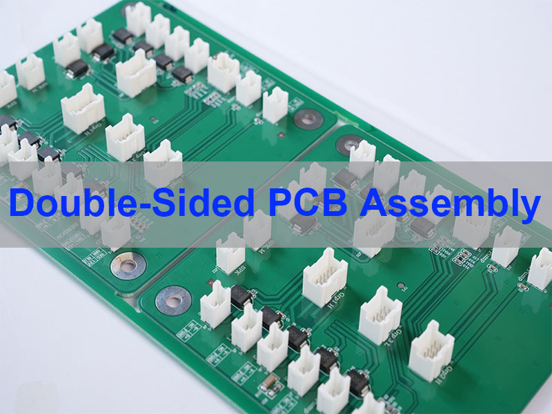
Double-Sided PCB Assembly Manufacturer | Custom Prototype to Mass Production
Double-sided PCB assembly is a manufacturing process where electronic components are mounted on both sides of a printed circuit board to achieve higher density, improved performance, and more efficient circuit design. This article explains how to optimize double-sided PCB assembly from process control to application reliability, helping you make better engineering and sourcing decisions.
EBest Circuit (Best Technology) is a professional double-sided PCB assembly manufacturer with 20 years of experience delivering stable, high-reliability PCBA solutions for global customers. We address common challenges such as inconsistent batch quality through strict process control and MES traceability, while our fast-turn manufacturing helps reduce lead times and keep your product launch on schedule. Our engineering team provides proactive DFM support to prevent redesign risks before production begins, and our integrated supply chain ensures consistent component sourcing and production stability. With certifications including ISO9001, ISO13485, and IATF16949, we maintain rigorous quality standards across every stage of production, ensuring your project is delivered with precision and reliability. A warm welcome to call us anytime at +84-827-237566 to get expert support for your double-sided PCB assembly project.
What Is Double-Sided PCB Assembly and Why Is It Widely Used?
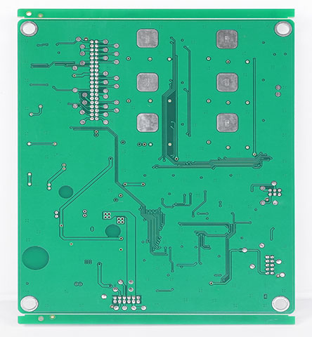
Double-sided PCB assembly refers to mounting components on both sides of a printed circuit board using SMT and/or through-hole processes. This approach significantly increases circuit density without increasing board size.
Key Benefits
- Higher integration density
- Improved electrical performance
- Reduced product size
- Better routing flexibility
Typical Applications
- Industrial control boards
- Power inverter systems
- UPS electronic circuits
- Communication modules
In practice, double-sided assembly enables compact designs while maintaining signal integrity and thermal balance.
How Does the Double-Sided PCB Assembly Process Work Step by Step?
The double sided pcb assembly process follows a controlled sequence to ensure component stability on both sides.
Step-by-Step Flow
- Solder paste printing (side A)
- SMT placement (side A)
- Reflow soldering (side A)
- Flip board and repeat process (side B)
- Through-hole insertion (if required)
- Wave or selective soldering
- Inspection (AOI + X-ray)
Critical Control Points
- Reflow temperature symmetry
- Component weight balancing
- Adhesive usage for heavy parts
As a result, process control directly impacts solder joint reliability and long-term product durability.
What Challenges Exist in Double-Sided SMT Assembly and How to Solve Them?
Double-sided SMT introduces complexity due to thermal cycles and gravity effects on components.
Common Challenges
- Component drop during second reflow
- Solder joint remelting
- Warping due to thermal stress
Our Solutions
- Optimized reflow profiles
- Use of SMT adhesive for critical parts
- Fixture support for large boards
From an engineering perspective, controlling thermal and mechanical stress is essential for maintaining assembly integrity.
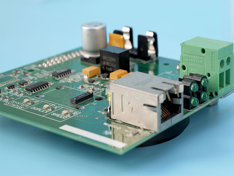
What Services Do We Provide for Double-Sided PCB Assembly?
We provide complete double-sided pcb assembly services from prototype to mass production.
Service Scope
- PCB fabrication
- SMT + THT assembly
- Mixed assembly (SMT + DIP)
- Functional testing
- Box build integration
Supported Variants
- Flex PCB double sided assembly
- Rigid-flex assembly
- High-density SMT assembly
Overall, integrated services simplify project management and improve production efficiency.
Our Certifications and Quality Assurance System
| Certification | Scope | Value |
|---|---|---|
| ISO 9001 | Quality Management | Consistent production control |
| ISO 13485 | Medical Devices | High reliability assurance |
| IATF 16949 | Automotive | Strict process standards |
| AS9100D | Aerospace | Advanced quality system |
Notably, certification-backed production ensures compliance, traceability, and long-term reliability.
What Problems Do Customers Face in Double-Sided PCB Assembly?
Many customers encounter recurring issues when sourcing double sided pcb assembly services.
Key Pain Points
- Unstable quality between batches
- Long lead time affecting product launch
- DFM issues causing redesign
- Supply chain inconsistency
How We Solve Them
- Full-process engineering support
- Stable MES-controlled production
- Component sourcing integration
- Fast prototype iteration
This means reliable partners reduce project risk and accelerate time-to-market.
What Industries Use Double-Sided PCB Assembly Most Frequently?
Double-sided PCB assemblies are widely used across high-demand industries.
Typical Industry Applications
- Industrial control: PLC and automation boards
- Power electronics: inverter electronic circuits
- UPS systems: backup power modules
- Telecommunication: signal processing boards
In real-world applications, these sectors require stable performance and long lifecycle reliability.
How Does Double-Sided PCB Assembly Compare with Single-Sided Assembly?
| Aspect | Double-Sided PCB | Single-Sided PCB |
|---|---|---|
| Component Density | High | Low |
| Routing Flexibility | Excellent | Limited |
| Assembly Complexity | Moderate | Low |
| Applications | Advanced electronics | Basic circuits |
In short, double-sided designs offer better performance and scalability for modern electronics.
How to Ensure High Yield in Double-Sided PCB Assembly Manufacturing?
double side pcb assembly manufacturing requires strict control over process variables.
Key Factors
- Stencil design optimization
- Accurate pick-and-place calibration
- Reflow profile tuning
- Inspection coverage (AOI + X-ray)
Best Practices
- DFM validation before production
- Controlled thermal cycles
- Use of high-quality solder paste
To sum up, yield improvement depends on both design optimization and process precision.
How Does Double-Sided PCB Assembly Support Inverter and UPS Applications?
Double side pcb assembly for inverter electronic circuit and UPS systems require high current handling and thermal stability.
Design Considerations
- Thick copper layers
- Thermal vias
- Balanced component placement
Assembly Focus
- Power component stability
- Heat dissipation control
- Mechanical reinforcement
Ultimately, proper assembly ensures stable operation under high load and thermal stress.
Why Choose a Reliable Double-Sided PCB Assembly Partner for Stable and Scalable Production?
Double-sided PCB assembly is the backbone of modern electronic manufacturing, enabling higher component density and better circuit routing compared to single-sided boards. Selecting a capable partner directly affects product stability, yield, and long-term reliability.
Core Parameters You Should Care About
- Minimum component size: 01005 / 0201
- Placement accuracy: ±30μm
- Layer alignment precision
- Double-sided SMT + THT compatibility
- Reflow profile control for both sides
Why Work With Us
- High yield through optimized process control
- Fast turnaround from prototype to volume
- Stable supply chain with traceability
- Engineering-driven DFM support
Therefore, choosing the right partner ensures manufacturability, consistent yield, and predictable product performance in real production environments.
Best Technology provides professional double-sided PCB assembly services from prototype to mass production. If you are looking for a reliable partner, pls feel free to contact us at sales@bestpcb.vn to start your project with Best Technology.
FAQs About Double-Sided PCB Assembly
Why use double sided pcb assembly instead of single sided?
It allows more components, better routing, and compact product design.
Can flex pcb double sided assembly be done?
Yes, with special handling and stiffeners to ensure structural stability.
Can you SMT solder components on both sides of a PCB?
Yes, this is a standard industry practice known as “Double-Sided SMT Assembly.” The process typically involves:
- Applying solder paste and placing components on the first side.
- Reflowing the first side in an oven.
- Flipping the board and repeating the process for the second side. Note: High-mass components on the first side may require specialized adhesives to prevent them from falling off when the board is inverted for the second reflow.
Is double-sided PCB assembly more expensive?
Generally, yes. Double-sided assembly is more costly than single-sided for several reasons:
- Increased Labor: The board must go through the SMT line twice.
- Stencils: You require two separate SMT stencils (one for the top, one for the bottom).
- Complex Testing: Automated Optical Inspection (AOI) and Flying Probe testing take longer because there are more test points and components to verify.
How do you prevent components from falling off during the second reflow?
Surface tension usually keeps smaller components in place when they are upside down during the second pass through the reflow oven. However, for heavy or bulky components, manufacturers use SMT glue (adhesive) to bond the component to the board before soldering. Additionally, engineers often design the board so that the lightest components are on the side that undergoes the second reflow.
Can double-sided PCBs use through-hole components?
Yes, but it adds complexity. While SMT components are preferred for double-sided designs, through-hole (THT) components can be used. This often requires wave soldering with a dedicated fixture (pallet) to protect the SMT components already on the bottom side, or selective soldering, which targets individual pins without affecting the rest of the board.
Overall, understanding these fundamentals helps improve design decisions and manufacturing outcomes.