 language
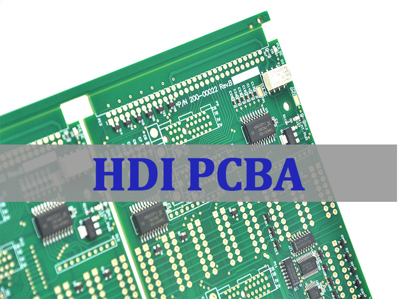
Custom HDI PCBA Manufacturer in Canada with Fast Delivery
HDI PCBA has become a critical solution for Canadian engineering teams developing compact, high-performance electronics that demand tight routing density, stable signal integrity, and reliable assembly execution. This article explains what HDI PCBA is, how custom HDI PCB PCBA assembly differs from traditional builds, what manufacturing capabilities matter most, and how to choose a reliable global partner that supports long-term scalability.
Modern Canadian hardware projects often face common challenges:
- Increasing signal speed and shrinking device size
- Limited local HDI fabrication capacity
- Long iteration cycles during prototyping
- Cost pressure without sacrificing reliability
- Need for global engineering collaboration
To address these engineering and supply-chain challenges, many teams adopt a more integrated HDI PCBA strategy that balances design flexibility, manufacturing capability, and global collaboration:
- High-density HDI stackup design and impedance control help support increasing signal speed while enabling smaller device footprints.
- Working with global HDI fabrication partners expands access to advanced materials and processes beyond limited local capacity.
- Rapid prototyping workflows with integrated PCB + PCBA shorten iteration cycles and accelerate validation builds.
- Transparent cost planning with DFM optimization reduces unnecessary rework and keeps reliability aligned with budget expectations.
- Engineering-led project coordination across regions ensures smooth communication between design teams and manufacturing partners worldwide.
As an established HDI PCBA manufacturer, EBest Circuit (Best Technology) delivers professional solutions tailored to real engineering needs, including DFM pre-review reports, BOM optimization lists, and practical process adaptation recommendations to improve manufacturability from the start. If you have any pertinent project requirements or would like to review our company profile first, please feel free to contact us at +84-827-237566 or sales@bestpcb.vn.
What Is HDI PCBA?
HDI PCBA refers to printed circuit board assembly based on High Density Interconnect structures, where microvias, fine line spacing, and advanced stackups enable higher routing density within smaller form factors. Compared with standard multilayer boards, HDI designs allow more components per area while maintaining electrical performance.
In practice, HDI PCBA is commonly used when:
- BGA pitch drops below 0.5 mm
- High-speed signals require impedance control
- Product size must be minimized
- Layer counts increase to support complex routing
Because HDI structures involve laser drilling and sequential lamination, the assembly process must be tightly aligned with the HDI PCB manufacturing process from the beginning.
Top 5 Custom HDI PCB PCBA Assembly Manufacturers in Canada
Canada hosts several capable electronics manufacturing service providers, although many focus more on assembly rather than advanced HDI fabrication. Engineering teams often evaluate partners based on HDI experience, engineering support, and scalability.
Typical examples of Canadian-based or Canada-focused suppliers include:
- Celestica – Known for aerospace and industrial electronics with strong global EMS infrastructure.
- Sanmina – Provides complex high-mix manufacturing and advanced PCBA integration.
- Creation Technologies – Offers design-for-manufacture support and industrial control PCBA solutions.
- Firan Technology Group (FTG) – Specialized in aerospace and high-reliability PCB solutions.
- Nortech Systems – Supports complex electronic assemblies with strong quality systems.
While these companies contribute to the local ecosystem, many Canadian engineering teams combine regional design expertise with overseas HDI PCB PCBA assembly partners to achieve faster lead times and higher layer-count flexibility.
How Does Custom HDI PCB PCBA Assembly Differ From Standard PCB Assembly?
Custom HDI PCB PCBA assembly introduces several technical differences compared with traditional PCB assembly:
- Microvias replace large mechanical vias to reduce routing congestion
- Fine line widths require precise solder paste printing and placement
- Sequential lamination affects thermal behavior during reflow
- Higher component density increases inspection complexity
Standard PCB assembly focuses primarily on throughput, while HDI assembly emphasizes precision and process discipline. For this reason, experienced HDI PCBA manufacturer teams integrate DFM review early to avoid yield issues during production.
What Manufacturing Capabilities Define a Reliable Custom HDI PCBA Manufacturer?
A strong HDI partner must go beyond basic SMT capability. Reliable suppliers typically provide:
- Laser drilling for microvias and stacked vias
- Fine pitch placement down to 01005 components
- Controlled impedance stackup validation
- AOI, X-ray, and functional testing
- Integrated PCB fabrication and assembly workflow
Engineering teams in Canada often prioritize partners who understand both fabrication and assembly stages, ensuring that design intent aligns with real manufacturing constraints.
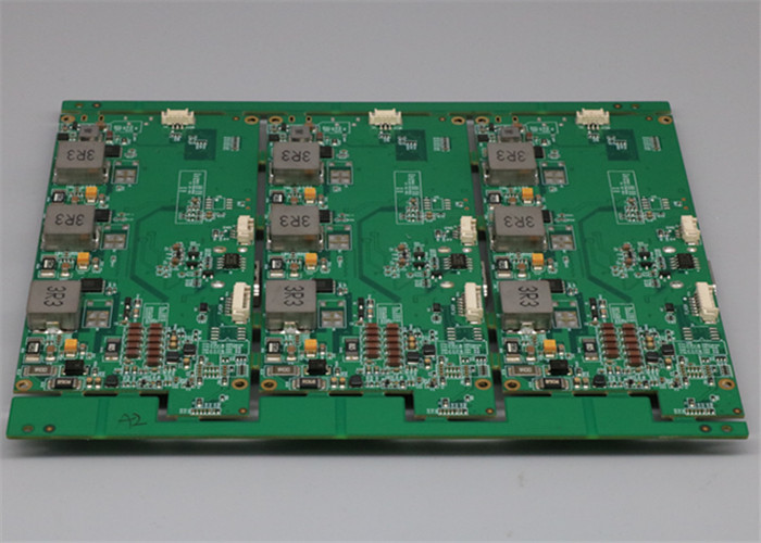
As a major custom HDI PCBA manufacturer, we have worked with leading Canadian medical and IoT brands to deliver tailored professional solutions. Below is an overview of our SMT capabilities for your reference.
| Item | Capabilities |
|---|---|
| Placer Speed | 13,200,000 chips/day |
| Bare Board Size | 0.2 x 0.2 inches – 20 x 20 inches / 22 * 47.5 inches |
| Minimum SMD Component | 01005 |
| Minimum BGA Pitch | 0.25mm |
| Maximum Components | 50 * 150mm |
| Assembly Type | SMT, THT, Mixed assembly |
| Component Package | Reels, Cut Tape, Tube, Tray, Loose Parts |
| Lead Time | 1 – 5 days |
What Is the HDI PCB Manufacturing Process Behind High-Density Designs?
The HDI PCB manufacturing process goes far beyond standard multilayer fabrication because high-density layouts require tighter control over microvia formation, layer registration, and copper distribution. For reliable HDI PCBA performance, fabrication must follow a structured sequence that ensures electrical integrity, stable impedance, and long-term reliability during assembly.
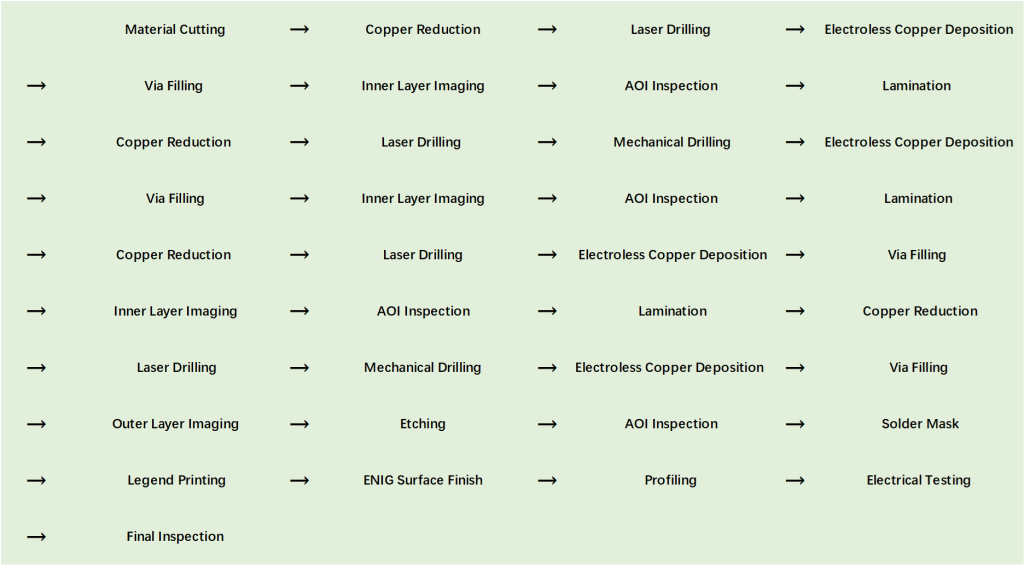
At EBest Circuit (Best Technology), HDI blind and buried via boards are produced through a controlled multi-cycle build process designed for production-intent designs rather than simplified prototypes. A typical workflow includes:
Material Preparation and Copper Optimization
Cutting panels → copper thinning to control impedance → preparation for laser microvia drilling.
Laser Microvia Formation and Metallization
Laser drilling → chemical copper deposition → via filling → inner layer imaging → AOI inspection.
Sequential Lamination Cycles
Multiple lamination stages are repeated to build stacked or staggered blind/buried vias while maintaining layer alignment and dielectric stability.
Precision Drilling and Outer Layer Formation
Mechanical drilling → copper plating → via filling → outer layer imaging → etching and inspection.
Surface Finishing and Final Validation
Solder mask application → legend printing → ENIG surface finish → profiling → electrical testing → final inspection.
A simplified representation of the internal HDI build flow is:
Each manufacturing stage must maintain strict dimensional and plating tolerances because even minor deviations can affect signal integrity, via reliability, and assembly yield. This disciplined process is why advanced HDI PCB products used in telecom infrastructure, automotive electronics, and aerospace systems depend on experienced HDI PCB + HDI PCB PCBA manufacturers capable of managing complex sequential builds from fabrication through assembly.
In practice, integrating HDI fabrication and assembly under one engineering workflow allows faster design feedback and more predictable results during high-density product development.
Why Do Canada Engineering Teams Source Custom HDI PCBA Globally Instead of Locally?
Although Canada offers strong design expertise, HDI fabrication capacity is more limited compared with Asia. Global sourcing provides several advantages:
- Access to mature supply chains and specialty materials
- Faster prototype turnaround cycles
- Competitive HDI PCB price structures
- Higher layer capability and advanced stackups
As a result, Canadian OEMs frequently collaborate with overseas partners who combine fabrication and assembly to shorten iteration loops while maintaining engineering control.
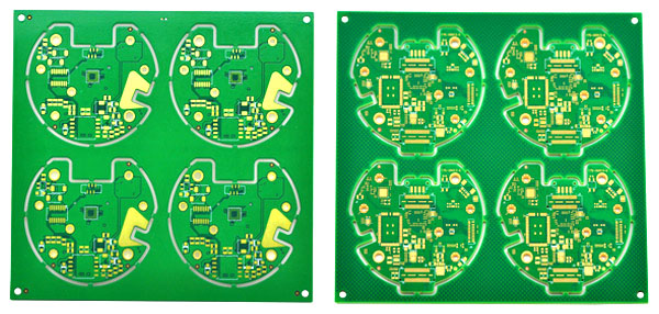
What Types of Products Commonly Use Custom HDI PCBA in Canada Projects?
HDI PCBA is widely used across Canadian technology sectors. Common applications include:
- Telecommunications and networking equipment
- Medical diagnostic electronics
- AI edge computing modules
- Industrial automation controllers
- Aerospace avionics systems
These products often require multilayer HDI structures to support high-speed signals, compact layouts, and thermal stability.
How Do HDI PCB Manufacturers Control Quality in High-Density Assembly?
Quality control in HDI builds must start during design validation. Leading HDI PCB manufacturer teams implement:
- Pre-production DFM and stackup review
- X-ray inspection for BGA and microvia reliability
- Flying probe electrical testing
- MES-based traceability for materials and process steps
These controls ensure that dense assemblies maintain long-term reliability under real operating conditions.
What Factors Influence Custom HDI PCBA Cost and Lead Time Planning?
Several elements determine overall project timelines and pricing:
- Layer count and stackup complexity
- Microvia structure and lamination cycles
- Component availability and sourcing strategy
- Testing requirements
- Volume and revision frequency
Unlike standard boards, HDI designs involve higher engineering involvement. However, efficient planning and integrated sourcing can stabilize cost and shorten delivery windows.
Why Choose EBest Circuit (Best Technology) as Your Custom HDI PCBA Partner for Canada Projects?
EBest Circuit (Best Technology) approaches HDI PCBA from an engineering-first perspective. Instead of focusing purely on volume production, the team emphasizes manufacturability, collaboration, and long-term scalability.
Key strengths include:
- Integrated PCB fabrication and HDI PCB PCBA assembly workflow
- Advanced HDI stackup support and high-layer capability
- Experienced engineers familiar with high-density routing challenges
- Flexible prototype-to-production transition
- Strong communication aligned with Canada engineering teams
With deep experience across complex hdi pcb products, EBest Circuit helps customers accelerate validation while maintaining stable production planning.
If you are planning a new HDI PCBA project or evaluating a reliable HDI PCBA manufacturer, EBest Circuit (Best Technology) provides engineering-driven support from prototype to production. For project discussions or inquiries, please contact us via sales@bestpcb.vn.
FAQs About HDI PCBA
Is HDI PCBA Suitable for Low-Volume Prototyping Before Mass Production?
Yes. Many Canada engineering teams use HDI PCBA for EVT, DVT, and pilot builds to validate signal integrity and thermal performance before scaling to volume production. Early HDI validation reduces redesign risk later.
What Files Are Required to Start an HDI PCBA Project?
Typical files include Gerber or ODB++, BOM list, centroid file, stackup details, and assembly drawings. Providing impedance targets early helps optimize the HDI PCB manufacturing process.
How Does HDI PCBA Affect Lead Time Compared With Standard PCBA?
HDI builds require additional lamination and laser drilling steps, which may extend fabrication time. However, integrated fabrication and assembly partners can shorten overall schedules.
Why Do Canada Companies Source HDI PCBA From Asia or Vietnam-Based Manufacturers?
Global partners offer stronger HDI infrastructure, faster iteration capability, and competitive pricing while maintaining engineering collaboration with Canada-based teams.