 language
PCB Panelization Guidelines for Assembly
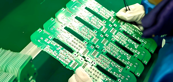
PCB panelization, or panelized PCB layout, is the process of combining multiple individual PCBs into a single larger panel. This enables automated assembly processes, reduces handling time, and improves production efficiency.
Panelization is particularly important for small, complex boards where manual handling would be inefficient or prone to errors.
Panel Requirements
PCB panelization is the process of combining multiple PCBs into a single panel or array to streamline manufacturing, assembly, and testing. Proper panel design ensures higher efficiency, better yields, and reduced costs.
The panel requirements are primarily dictated by the PCB assembly process, the manufacturing capabilities, and the end-product specifications. Key considerations include:
- Panel Size: Standard panel sizes are often based on the capabilities of pick-and-place machines, reflow ovens, and wave soldering lines. Typical panel dimensions range from 300×400 mm to 460×610 mm, though custom sizes may be required for specific equipment.
- Material Thickness: Panels usually retain the same base material as the individual PCB but must maintain flatness to prevent soldering or assembly defects.
- Edge Clearance: Maintain sufficient clearance at the panel edges to allow tooling, handling, and depanelization without damaging the boards.
- Fiducial Marks: Include fiducial marks on each PCB for accurate alignment during automated assembly. At least three fiducials per PCB are recommended, ideally one on each corner or per orientation axis.
- Routing and Breakaway Tabs: Decide between V-scoring or tab-routing to separate boards after assembly. Tabs must be strong enough to hold the panel together during handling but easy to break after production.
Properly meeting panel requirements is essential for preventing assembly errors and optimizing throughput.
PCB Panelization Guidelines for Assembly
1. Fiducial Placement
Fiducial marks help machines locate components and align boards accurately. Recommended practices:
- Include three fiducials per PCB: two along one diagonal and one offset on the opposite side.
- Fiducials should be at least 1.5 mm in diameter with a minimum 0.5 mm clearance from any copper or solder mask.
2. Breakaway Tabs and V-Scoring
There are two main methods for depanelization:
- V-Scoring: Ideal for simple shapes. V-shaped grooves are scored on both sides of the PCB. After assembly, boards can be snapped apart easily. Ensure corner radius ≥ 1 mm to avoid stress points.
- Tab-Routing: Used for complex shapes. Small tabs hold the PCB in place during assembly. Tabs are later cut or broken. Design with 3–6 tabs per edge, depending on panel size and component placement.
3. Tooling Holes and Mouse Bites
Tooling holes allow panels to be accurately positioned in assembly equipment. Best practices include:
- Use 0.8–1.2 mm diameter holes.
- Place holes near panel corners and along the edges to ensure mechanical stability.
- Mouse bites are small perforations along tabs to allow easy separation. Maintain a spacing of 1.0–1.5 mm between bites.
4. Copper Keep-Out Areas
To avoid soldering issues, maintain a minimum copper keep-out area around the edge of panels and around tooling holes. Typically, 1–1.5 mm of clearance is sufficient to prevent shorts or solder bridging.
5. Panel Markings
Include panel-level markings for traceability and inspection:
- PCB part number and revision
- Date code or lot number
- Assembly or customer identifier
- Orientation indicators
6. Thermal Considerations
Large copper areas or uneven copper distribution can lead to warping during reflow soldering. To minimize this:
- Use thermal relief patterns for pads connected to large copper pours.
- Balance copper density across the panel.
- Consider using panel stiffeners or a thicker base material for very large panels.
7. Keep Assembly Constraints in Mind
Panel design must consider the pick-and-place equipment, reflow oven width, and handling processes. For example:
- Avoid placing components too close to the panel edge (<5 mm), as this can cause misalignment.
- Keep similar components together to improve machine efficiency.
- Ensure sufficient clearance for test probes and inspection cameras.
9 Key Considerations for PCB Panelization
Below are the 9 essential guidelines for effective PCB panelization:
1. Closed-Loop Panel Frame:
The outer frame of the panel should form a closed loop to keep the panel fixed on fixtures without warping during assembly.
2. Panel Shape:
Panels should be as square as possible. Typical layouts are 2×2, 3×3, or similar grids. Avoid creating uneven board shapes, which can cause handling issues.
3. Panel Size:
- Width ≤ 260 mm for SIEMENS lines or ≤ 300 mm for FUJI lines.
- For automated dispensing, panel width × length ≤ 125 mm × 180 mm.
4. Positioning Holes for Sub-Boards:
- Each sub-board should have at least three positioning holes.
- Hole diameter: 3–6 mm.
- No routing or component placement within 1 mm of edge positioning holes.
5. Spacing Between Boards:
Maintain center-to-center distance between sub-boards at 75 mm–145 mm to allow for depanelization and handling.
6. Reference Fiducial Zones:
When setting reference points for alignment, leave a 1.5 mm solder-free area around fiducials to prevent solder bridging or component interference.
7. Component Placement Near Panel Edges:
- Avoid placing large or protruding components near the panel edge or frame.
- Maintain ≥0.5 mm spacing between components and PCB edges to ensure cutting tools operate correctly.
8. Corner Tooling Holes:
- Drill four corner holes on the panel frame, diameter 4 mm ± 0.01 mm.
- Holes must be strong enough to withstand handling but precise in position and smooth in the hole wall to prevent damage during assembly.
9. Sub-Board Fiducials and Positioning Symbols:
- QFP components with spacing < 0.65 mm should have fiducials on diagonal corners.
- Sub-board reference symbols should be used in pairs at opposite diagonal positions.
- Large components such as I/O interfaces, microphones, battery connectors, switches, earphone jacks, or motors should include dedicated positioning pins or holes.
FAQs
1. What is the purpose of PCB panelization?
It allows multiple boards to be manufactured and assembled together, improving efficiency and reducing handling errors.
2. How many positioning holes are needed per sub-board?
At least three positioning holes per sub-board, with a diameter of 3–6 mm.
3. Can components be placed near the panel edge?
Components should be at least 0.5 mm from the panel edge to prevent interference with cutting or depanelization.
4. What is the recommended panel shape?
Panels should be close to square, typically arranged in 2×2 or 3×3 grids, avoiding irregular shapes.
5. Why leave solder-free zones around fiducials?
A 1.5 mm solder-free zone prevents solder bridging and ensures accurate alignment for automated pick-and-place machines.