 language
Through-Hole Assembly
Through hole assembly is a time-tested PCB assembly technique that continues to play a significant role in today’s electronics manufacturing world. Even with the widespread adoption of surface mount technology (SMT), through-hole assembly remains indispensable in applications demanding mechanical strength, high reliability, or where components experience physical stress.
What Is Through-Hole Assembly?
Through-hole assembly is a traditional PCB manufacturing process where component leads are inserted into drilled holes on the board and soldered to pads on the opposite side. This forms a robust mechanical and electrical connection between the component and the PCB.
Unlike surface-mount components that rest on the surface of the board, through-hole components penetrate through it. This physical anchoring provides higher durability, especially in applications that face vibration, heat, or mechanical stress.
The process typically involves several steps:
1. Drilling: Holes are drilled based on the component lead diameter.
2. Component Insertion: Operators or automated insertion machines place the components.
3. Soldering: The solder joints are formed either manually or through wave soldering.
4. Inspection: The board is visually or automatically inspected for quality assurance.
Through-hole assembly is particularly suitable for prototypes, large components, and mission-critical devices where connection reliability outweighs compactness.
Why Use Through-Hole Assembly?
Even with today’s shift toward miniaturized electronics, through-hole assembly still holds a strong place in PCB manufacturing. It’s not about being old-fashioned — it’s about reliability. When your design needs strength, durability, and consistent performance under stress, through-hole mounting steps in.
1. Exceptional Mechanical Strength
Through-hole components are literally anchored into the board. Their leads go through drilled holes and are soldered on the other side, creating a solid bond that can handle vibration, shock, or physical stress. That’s why you’ll still find them in aerospace systems, industrial machinery, and automotive controls where parts can’t afford to come loose.
2. Better Heat Resistance
Because the leads go through the PCB, heat transfers more effectively away from the component body. This makes through-hole components great for circuits that run hot — like power converters, amplifiers, or high-current sections. They can handle temperature changes without cracking or detaching.
3. Ideal for Prototyping and Testing
When engineers are still fine-tuning a design, through-hole components make life easier. They’re easier to plug in, remove, or replace compared to tiny surface-mount parts. You can test, measure, and adjust without needing reflow equipment — perfect for early-stage development.
4. Strong Support for Larger Components
Some components are just too bulky or heavy for surface mounting. Think of transformers, connectors, or electrolytic capacitors — these parts need extra physical support. Through-hole mounting keeps them firmly in place even in rugged operating environments.
5. Works Well in Hybrid Designs
Modern PCBs often combine the best of both worlds. You might use SMT for compact logic circuits and through-hole for connectors or power devices. This hybrid approach keeps the board small but still robust in critical areas.
So, while surface mount technology dominates small-scale electronics, through-hole assembly continues to shine wherever strength, reliability, and repairability matter most.
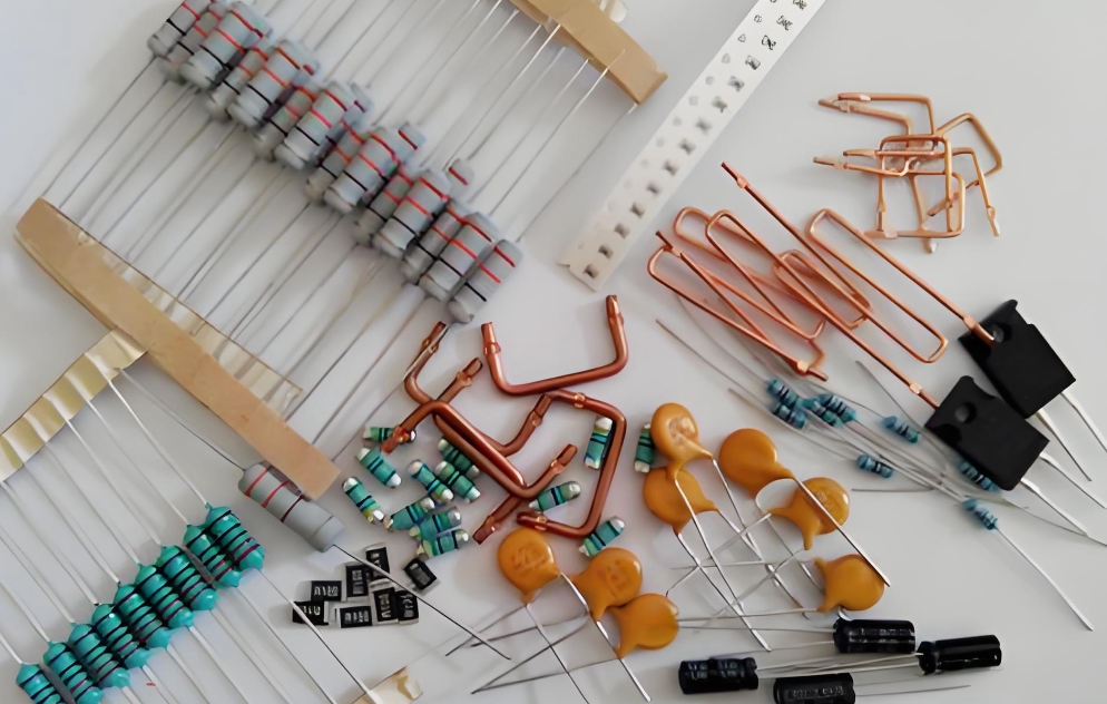
Common Through-Hole Component Types
Through-hole components come in various forms and package styles. Here are the most frequently used categories in PCB assembly:
1. Axial Lead Components
Axial components have leads extending from both ends of the body, parallel to the component’s central axis. They lie flat on the PCB surface, making them suitable for compact layouts. Typical examples include resistors, diodes, and some capacitors.
2. Radial Lead Components
In radial components, both leads exit from one side of the component body. These parts stand vertically on the PCB, saving horizontal space. Common radial parts include electrolytic capacitors and some types of LEDs.
3. Dual Inline Package (DIP)
DIP components are rectangular packages with two parallel rows of pins. They are used for ICs, relays, and connectors. These components can be inserted manually or via automatic insertion equipment.
4. Transistors and Power Devices
Transistors, voltage regulators, and power MOSFETs often use through-hole packaging for heat dissipation and current handling. TO-220 and TO-92 are common package styles.
5. Connectors and Transformers
These large components require mechanical stability and strong anchoring, which through-hole assembly provides effectively.
Each type of component offers distinct benefits depending on electrical performance, board layout, and mechanical requirements.
Through-Hole Assembly Design Considerations
Designing a PCB for through-hole assembly involves more than just drilling holes. Several factors influence manufacturability, soldering quality, and long-term reliability.
1. Hole Size and Tolerance
The hole diameter should be slightly larger than the component lead, allowing for easy insertion and proper solder flow. Standard tolerances are around +0.1 mm, but exact values depend on plating and board thickness.
2. Pad Design
Pads must be large enough to ensure adequate solder fillet formation without risking bridging. Insufficient pad size can weaken joints, while overly large pads may cause solder imbalance.
3. Component Spacing
Allowing enough clearance between components prevents thermal interference and simplifies soldering. Adequate spacing also facilitates inspection and repair.
4. Plated Through Holes (PTH)
For double-sided or multilayer boards, plated through holes provide conductivity between layers. Proper plating thickness (usually 25–35 µm) ensures consistent electrical performance and mechanical strength.
5. Wave Soldering Orientation
When using wave soldering, components should be aligned to minimize shadowing effects. Grouping similar component types can improve solder uniformity.
6. Thermal Relief Pads
For large copper planes, thermal relief connections help control heat flow during soldering, preventing cold joints.
A well-thought-out design minimizes production issues and leads to better yield and quality.
Through-Hole Assembly vs. Surface Mount Assembly
The debate between through-hole and surface mount assembly often centers on performance, cost, and application scope. Both technologies have their strengths.
| Feature | Through-Hole Assembly | Surface Mount Assembly |
| Mounting Style | Component leads go through drilled holes | Components soldered on PCB surface |
| Mechanical Strength | Very strong and durable | Moderate, depends on pad adhesion |
| Component Density | Lower | Higher, suitable for compact designs |
| Automation | Partially automated | Fully automated |
| Repair & Prototyping | Easier | More challenging |
| Thermal Performance | Better heat dissipation | Limited by pad contact area |
| Cost Efficiency | Higher labor and drilling cost | Lower for mass production |
Surface mount assembly dominates in miniaturized electronics such as smartphones, but through-hole remains unmatched in high-reliability and power applications.
Many designs today use a hybrid approach—combining SMT for compactness and through-hole for mechanical or thermal performance.
Common Defects in Through-Hole Assembly
Even with careful design and process control, through-hole assembly can sometimes run into a few quality issues. Most of them come down to soldering conditions, material handling, or improper hole design. Knowing these common defects helps engineers spot problems early and improve yield.
1. Insufficient Solder Fill
This happens when solder doesn’t completely fill the plated hole, leaving gaps that weaken the joint. It usually points to issues like low solder temperature, incorrect flux application, or contamination on component leads. When solder can’t flow properly, the connection loses both strength and conductivity.
2. Cold Solder Joints
Cold joints are easy to recognize — the surface looks dull or grainy instead of smooth and shiny. They form when the solder isn’t heated enough to create a proper metallurgical bond. Over time, these joints may develop cracks or high resistance, especially under vibration.
3. Solder Bridging
When too much solder accumulates, it can flow between adjacent pins and cause an unintended electrical connection. This short circuit can damage components or make the circuit unstable. Controlling solder volume and wave angle during wave soldering usually prevents this issue.
4. Component Misalignment
If components are not inserted straight or at the correct depth, they can tilt or sit unevenly. Misaligned parts not only look unprofessional but also create stress points on the leads. Proper fixturing and insertion tooling can help maintain uniform placement.
5. Lifted Pads or Traces
Excessive heat or repeated soldering can cause the copper pad to separate from the PCB surface. Once lifted, it’s difficult to repair without damaging nearby traces. Using the right soldering temperature and avoiding prolonged contact with the iron keeps pads intact.
In most cases, these problems can be prevented through process optimization, consistent operator training, and detailed inspection. Automated Optical Inspection (AOI) or X-ray analysis also plays a big role in catching defects early before the board moves to the next stage.
Through-Hole Assembly Fabrication Notes
Successful through-hole fabrication depends on precise coordination between design, materials, and process control. Here are essential guidelines manufacturers often follow:
1. Component Lead Length: Leads should protrude 0.5–1.5 mm from the solder side for optimum wetting.
2. Board Thickness: Thicker boards require proper preheating to ensure full solder penetration.
3. Flux Application: Uniform flux coverage helps prevent oxidation and promotes solder flow.
4. Wave Height and Angle: In wave soldering, maintaining consistent solder wave parameters ensures uniform joints.
5. Cleaning: Residual flux should be removed to prevent corrosion and electrical leakage.
6. Inspection Standards: IPC-A-610 is typically referenced for through-hole solder joint acceptance criteria.
Following these process notes helps maintain consistency and reliability across production batches.
Why Partner with Best Technology for Through-Hole PCB Assembly?
When you need reliable through-hole PCB assembly, Best Technology delivers both precision and performance. Our facilities are equipped to handle single-sided, double-sided, and hybrid SMT + THT assemblies, supported by advanced wave soldering and AOI inspection systems.
Whether used alone or in combination with SMT, through-hole assembly provides the solid foundation that many industries still rely on. And with a trusted manufacturing partner like Best Technology, you can count on precision workmanship, consistent quality, and dependable support throughout every stage of your PCB production.
With competitive pricing, professional support, and fast turnaround, Best Technology helps customers bring robust and dependable electronics to market faster.