 language
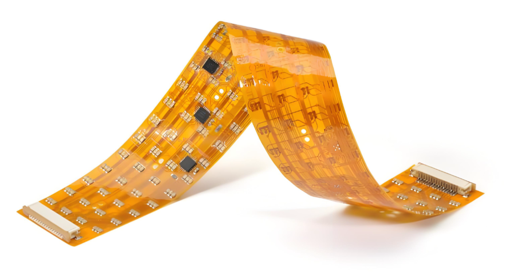
Flex PCB Assembly
Flex PCB assembly is transforming the way electronic devices are designed and manufactured. As products get smaller and more powerful, the demand for flexible, lightweight, and space-efficient circuit solutions continues to rise. From wearable devices and medical instruments to automotive systems and aerospace electronics, flexible circuits enable design possibilities that rigid boards simply cannot match.
What Is a Flexible PCB?
A flexible PCB (Printed Circuit Board), often called a flex circuit, is a type of circuit board built on a bendable base material like polyimide (PI) or polyester (PET) instead of a rigid fiberglass substrate.
Flex PCBs are constructed using thin copper foil laminated onto the flexible substrate, forming conductive traces that remain stable even under mechanical stress. They are lightweight, compact, and can replace multiple rigid boards connected by cables, reducing interconnect complexity and improving reliability.
The flexibility of the board does not just mean physical bending — it also represents design freedom, enabling electronic systems to fit in tight spaces without sacrificing electrical performance.
Flex PCB Types
Flexible PCBs come in several configurations based on their layer structure and intended functionality. Here are the most common types:
| Type | Description | Typical Use |
| Single-Sided Flex PCB | Has one conductive copper layer on a flexible substrate. | Simple interconnects, printers, and consumer electronics. |
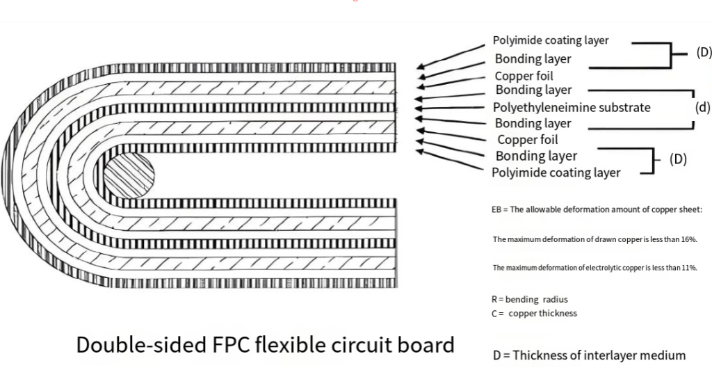
| Double-Sided Flex PCB | Contains copper layers on both sides of the base material, connected by vias. | More complex circuits and higher-density routing. |
| Multilayer Flex PCB | Includes three or more copper layers separated by insulating dielectric films. | High-performance applications like medical imaging and aerospace systems. |
| Rigid-Flex PCB | Combines rigid and flexible sections in a single design. | Devices requiring both durability and foldable sections, such as cameras or smartphones. |
| Sculptured Flex PCB | Uses variable copper thickness for areas needing high current capacity or mechanical strength. | Power electronics and high-current devices. |
Each type serves different needs — from ultra-thin wearable sensors to advanced military control systems — offering engineers wide design flexibility.
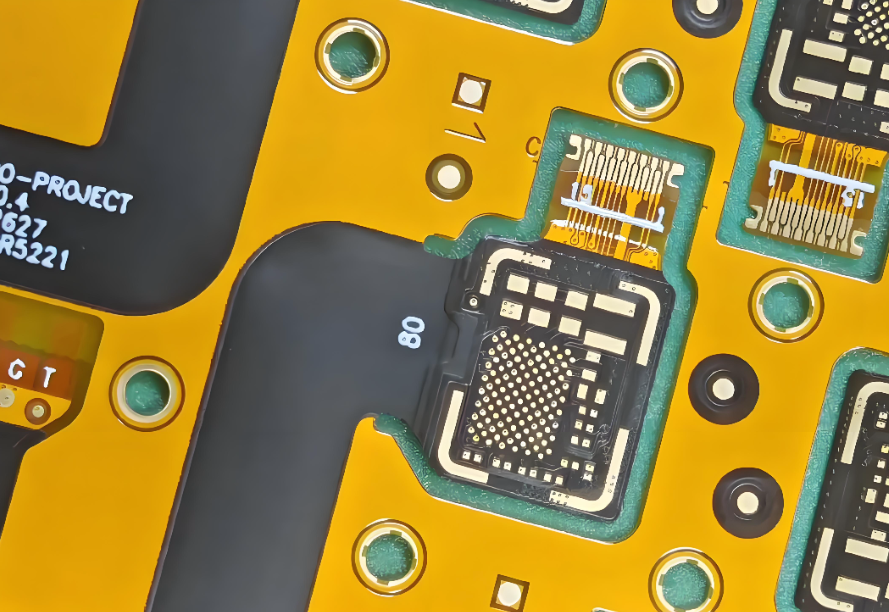
Flexible PCB Assembly Process
The flex PCB assembly process involves multiple precise steps to ensure both flexibility and functionality are maintained throughout production. Unlike rigid boards, flex circuits require extra care to handle delicate materials and avoid damage during soldering.
Below is the general process flow for assembling flex PCBs:
| Step | Description |
| 1. Material Preparation | Clean and prepare polyimide base and copper foil to remove contaminants. |
| 2. Circuit Imaging & Etching | Photoresist patterning and chemical etching to create circuit traces. |
| 3. Drilling & Plating | Laser or mechanical drilling of vias followed by electroless copper plating. |
| 4. Solder Mask & Surface Finish | Apply solder mask for protection and finishes like ENIG or OSP for solderability. |
| 5. Component Placement | Using pick-and-place machines for SMD components or manual placement for delicate parts. |
| 6. Reflow or Hand Soldering | Controlled soldering under temperature profiles safe for flexible materials. |
| 7. Inspection & Testing | AOI, X-ray, and electrical testing to ensure functionality and reliability. |
| 8. Final Forming | Folding or shaping the flex circuit according to product design. |
Temperature control and handling precision are critical throughout the process. Excessive heat can damage the polyimide substrate, while improper handling may cause microcracks or trace separation.
Design Considerations for Flex PCB Assembly
Designing a flex PCB assembly requires a balance between mechanical flexibility and electrical reliability. Unlike rigid PCBs, flexible circuits must bend and twist repeatedly without causing copper fatigue or delamination. A successful flex PCB design begins with understanding the unique behavior of flexible materials, copper thickness, and assembly processes. Every design decision—from trace routing to component placement—can directly impact long-term performance.
Let’s look at the key design considerations that engineers should always keep in mind:
1. Bending Radius and Flexibility Zones
One of the most critical factors in flex PCB design is the minimum bending radius. If the bend radius is too tight, the copper traces may crack or delaminate. As a general rule, the minimum bend radius should be at least 10 times the overall board thickness for dynamic applications (those that flex frequently) and 5 times the thickness for static applications (those that bend only during installation).
It’s also important to define flex zones — areas designed to bend — and stiff zones, which hold components. Avoid placing vias, solder joints, or heavy components in flex zones. These regions experience continuous mechanical stress, which can cause premature failures.
2. Trace Routing and Pad Design
The routing of copper traces plays a major role in maintaining circuit integrity. Sharp corners and 90° angles should be avoided, as they create stress concentration points during bending. Instead, use curved or teardrop-shaped traces, which distribute stress evenly across the conductor.
Pads for surface-mount components should also have anchor spurs or teardrops to prevent lifting during soldering or bending. For high-density interconnect (HDI) designs, using filleted pad edges helps strengthen the connection between copper and polyimide base material.
3. Copper Thickness and Material Selection
The thickness of the copper foil determines both the electrical performance and the flexibility of the circuit. Thicker copper offers better current-carrying capacity but reduces flexibility, while thinner copper improves bending ability but limits current flow.
For most flexible designs, 1 oz (35 μm) or ½ oz (18 μm) copper is used. For dynamic flex circuits—like those in wearable devices—⅓ oz (12 μm) copper is ideal, as it withstands repetitive bending without fatigue.
4. Stiffeners and Support Structures
Since flexible PCBs cannot support components on their own, stiffeners are often added to reinforce specific areas. These are usually made of FR-4, polyimide, or stainless steel and placed under connectors, ICs, or other heavy components to provide mechanical support during assembly.
5. Coverlay vs. Solder Mask
Traditional PCBs use a solder mask, but flexible circuits require polyimide coverlay instead. Coverlays act as insulation and mechanical protection while still allowing flexibility.
The adhesive and thickness of the coverlay must be chosen carefully. Too thick, and it reduces flexibility; too thin, and it won’t protect the copper adequately. Openings in the coverlay for solder pads should have smooth, rounded edges to avoid stress risers and tearing during flexing.
6. Via Placement and Hole Design
Vias in flexible circuits are more vulnerable to stress compared to rigid boards. To enhance reliability, avoid placing vias directly in the bend area. Instead, move them to stiffened or non-flexing sections.
When vias are necessary near a bend, use teardrop transitions and larger annular rings to reinforce the area. For multilayer flex designs, staggered via placement helps prevent stress alignment across layers.
7. Thermal Management
Even though flex PCBs are thinner than rigid ones, they still need effective thermal control. Polyimide has lower thermal conductivity than FR-4, so heat from components must be managed carefully.
Designers can use copper pour planes, thermal vias, or heat-spreading films to dissipate heat efficiently. In power or LED applications, consider stiffeners with metal cores to improve heat transfer away from hot components.
Characteristics of Flex PCB Assembly
Flex PCB assemblies exhibit several distinctive characteristics that make them superior for certain applications:
- Lightweight Construction: Ideal for portable and miniaturized devices.
- Dynamic Flexibility: Can withstand continuous bending and movement cycles.
- High Heat Resistance: Polyimide base material tolerates high-temperature soldering.
- Space Efficiency: Reduces the need for connectors and cables.
- Improved Signal Integrity: Shorter interconnections reduce noise and signal loss.
- Enhanced Reliability: Fewer solder joints mean fewer potential failure points.
Differences Between Flex PCB Assembly and Rigid Assembly
Although both technologies serve the same purpose—connecting electronic components—their materials, structure, and handling requirements differ significantly.
| Aspect | Flex PCB Assembly | Rigid PCB Assembly |
| Base Material | Polyimide or polyester | FR-4 (fiberglass epoxy) |
| Flexibility | Can bend and fold | Completely rigid |
| Weight | Very lightweight | Heavier |
| Assembly Process | Requires careful temperature and handling | More straightforward soldering |
| Design Freedom | Allows complex 3D shapes | Limited to flat layouts |
| Durability | Excellent under vibration or movement | Better for static installations |
| Cost | Slightly higher due to specialized materials | Lower for mass production |
The choice between flex and rigid PCB assembly depends on application requirements. For compact, movable, or wearable devices, flex PCBs are unmatched. However, for cost-sensitive or static products, rigid boards remain more economical.
Tests of Flex Circuit Assemblies
Quality assurance is vital in flex PCB production because the materials are thinner and more sensitive. Testing ensures that every flex circuit meets performance, reliability, and safety standards. Here are the most common testing methods:
- Electrical Testing: Verifies circuit continuity and insulation resistance.
- Bend/Flex Test: Repeated bending under controlled conditions to assess mechanical durability.
- Thermal Cycling Test: Simulates high and low temperature exposure to test solder joint reliability.
- Impedance Testing: Ensures consistent signal transmission in high-speed designs.
- Visual and AOI Inspection: Detects defects like solder bridges, misaligned components, or trace breaks.
- X-ray Inspection: Used for verifying internal layers, hidden solder joints, or BGAs.
Only boards that pass all these inspections move forward to packaging and shipment.
Applications of Flex PCB Assembly
Flex PCB assemblies are used across industries where space optimization, lightweight structure, and reliability are essential. Some key application areas include:
- Consumer Electronics: Smartphones, cameras, wearable fitness devices, and foldable displays.
- Medical Equipment: Pacemakers, hearing aids, and diagnostic sensors.
- Automotive Systems: Airbag sensors, dashboard displays, and infotainment units.
- Aerospace & Defense: Satellites, radar systems, and missile guidance electronics.
- Industrial Automation: Flexible sensors, control systems, and robotic joints.
Flex PCBs continue to enable the next generation of miniaturized, high-performance electronic devices.
Why Choose Best Technology for Flex PCB Assembly?
When it comes to flex PCB assembly, precision and quality control are everything. At Best Technology, we combine engineering expertise with advanced manufacturing capabilities to deliver superior flexible circuits tailored to your requirements.
Our advantages include:
- Various flexible PCB types like single sided, multilayer, rigid-flex PCB, FFC fabrication
- Over 19 years with mature manufacturing techniques
- ISO9001, ISO13485, IATF16949, and AS9100D
- Full tracking from raw material to finished product
- AOI, X-ray, and functional testing for every assembly.
- DFM review and DFA free checks before production
Choosing Best Technology means partnering with a team that not only understands the technology but also helps you transform complex designs into reliable, high-performance products.
FAQs About Flex PCB Assembly
1. What is the typical lead time for a flex PCB assembly project?
Lead time usually ranges from 10 to 20 working days, depending on board complexity, quantity, and component sourcing. Quick-turn options are available.
2. Can flex PCBs be combined with rigid sections?
Yes. Rigid-flex PCBs are designed to integrate both technologies, offering durability in rigid areas and flexibility where bending is needed.
3. What materials are used for flexible PCB substrates?
Common materials include polyimide (PI) and polyester (PET), with polyimide being preferred for high-temperature and high-performance applications.
4. How durable are flex circuits under repeated bending?
Well-designed flex PCBs can withstand tens of thousands of bending cycles without failure, depending on the bend radius and copper thickness.
5. How does Best Technology ensure the quality of flex PCB assemblies?
Every board undergoes AOI, electrical testing, impedance measurement, and visual inspection before shipment. Strict adherence to ISO and IPC standards guarantees consistent performance.
At Best Technology, we don’t just assemble flexible PCBs — we help engineers build the future of electronics. Our expertise, certifications, and customer-focused approach ensure every flex PCB assembly meets the highest global standards for quality and reliability.
If you’re ready to turn your innovative design into a flexible, production-ready solution, contact Best Technology today — your trusted partner in advanced PCB manufacturing.