 language
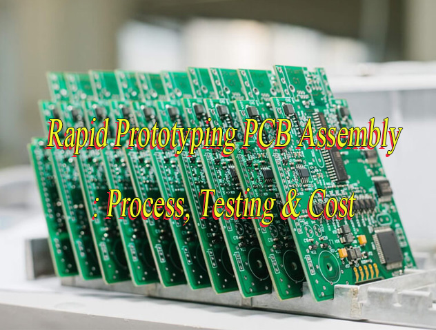
Rapid Prototyping PCB Assembly: Process, Testing & Cost
Rapid prototyping PCB assembly is a streamlined process that delivers functional PCB prototypes quickly, enabling fast design validation and iteration. Unlike traditional PCB assembly, rapid prototyping PCB assembly prioritizes speed without compromising basic quality, making it ideal for testing new designs before full-scale production. It combines efficient component sourcing and simplified assembly techniques to reduce lead times, helping bring products to market faster while controlling initial development costs.
What Is Rapid Prototyping PCB Assembly?
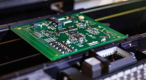
Rapid prototyping PCB assembly is the expedited process of populating bare PCBs with electronic components to create functional prototypes. Its core goal is to reduce the time from design finalization to a testable prototype, often delivering results in days rather than weeks. This speed is achieved by optimizing every step of the assembly process, from component sourcing to final testing.
This process combines efficient component sourcing, streamlined assembly techniques and basic quality checks to produce prototypes that accurately reflect the final product’s functionality. Rapid prototyping PCB assembly focuses on small-batch production, making it cost-effective for design iteration and validation. It allows for quick adjustments to designs based on prototype testing, minimizing the risk of costly errors in mass production.
Rapid Prototyping PCB Assembly Process
- Design Finalization and DFM Check: Review PCB design files and perform Design for Manufacturability checks to ensure compatibility with assembly processes, minimizing rework requirements and avoiding assembly conflicts.
- BOM Preparation: Create a detailed bill of materials with exact part numbers quantities and alternative components to facilitate easy sourcing during rapid prototyping PCB assembly.
- Component Sourcing: Source required components promptly prioritizing component availability to prevent delays in the assembly timeline and keep the prototyping process on track.
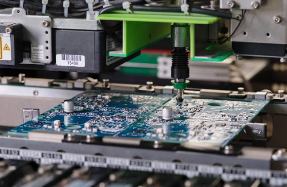
- Solder Paste Application: Apply solder paste to PCB pads using a precision stencil to ensure consistency a critical step for forming reliable connections with surface-mount components.
- Component Placement: Accurately place components on PCB pads and utilize semi-automated placement tools to ensure precision for small-batch rapid prototyping PCB assembly.
- Soldering: Use reflow ovens for surface-mount components or manual wave soldering for through-hole parts to form secure stable electrical connections that meet basic quality standards.
- Initial Inspection: Perform visual inspections to identify visible defects such as misaligned components or insufficient solder ensuring basic assembly quality before moving to testing.
- Basic Functional Testing: Conduct basic functional testing to verify the prototype operates as intended confirming the success of rapid prototyping PCB assembly and validating the initial design.
SMT vs. THT for Rapid Prototyping Printed Circuit Board Assembly
- Application Suitability: SMT is ideal for compact, high-density prototypes with small surface-mount components, offering higher assembly density and smaller product size which is perfect for miniaturized designs. THT performs better for prototypes with larger through-hole components, such as connectors or power devices, and is preferred for high-mechanical-stress applications where component stability is critical.
- Assembly Speed: SMT is significantly faster for rapid prototyping PCB assembly thanks to automated placement equipment that enables high-precision, batch component mounting. THT often relies on manual soldering, which slows down the process, making it more suitable for small quantities of prototypes with special through-hole components.
- Cost Efficiency: SMT has lower labor costs for small-batch prototypes due to automated operations, though it requires a one-time investment in specialized stencils that can be reused. THT has lower initial setup costs as it does not need stencils, with manual soldering keeping labor costs manageable for small-volume rapid prototyping.
- Component Compatibility: SMT supports smaller, more advanced components (such as 0402, 0201 package parts) and high-density layouts, aligning with modern prototype design needs. THT is compatible with older, larger components or those that cannot be surface-mounted, including traditional DIP packages and high-power through-hole parts.
- Reliability: THT provides stronger mechanical bonds between components and PCBs, making it suitable for prototypes used in harsh environments with vibration, high temperature or humidity. SMT delivers reliable electrical connections for standard applications in rapid prototyping PCB assembly, excelling in high-density layouts without compromising basic performance.
How to Select Components for Rapid Prototyping PCB Assembly?
- Prioritize Standard Components: Choose commonly used packages like 0402, 0603, or SOIC for rapid prototyping PCB assembly. These standard packages are readily available from most distributors, eliminating delays from sourcing hard-to-find specialty components and ensuring compatibility with standard assembly equipment.
- Check Component Availability: Select components with lead times of 3 days or less to keep rapid prototyping PCB assembly on schedule. If primary components are out of stock or have long lead times, pre-approve 1-2 functionally identical alternatives to avoid costly delays.
- Match Component Specifications: Select components that exactly meet the prototype’s electrical (voltage, current, resistance) and thermal (power rating, operating temperature) requirements. Avoid over-specifying as using a higher-rated component than needed only increases costs without adding value to prototype testing.
- Consider Assembly Compatibility: Align components with your chosen assembly method (SMT or THT) for rapid prototyping PCB assembly. For SMT, choose surface-mount packages with standard footprints; for THT, select through-hole components with standard pin spacing to minimize rework and defects.
- Optimize for Cost-Effective Options: Choose budget-friendly, reliable components for prototypes as they will be replaced with production-grade parts later. Avoid premium brands or custom components for prototyping, as they unnecessarily drive up initial development costs without improving testing outcomes.
What Testing Methods Work for Rapid Prototyping PCB Board Assembly?
Testing Methods for Rapid Prototyping PCB Assembly:
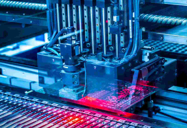
- Automated Optical Inspection (AOI): Based on optical principles, this method uses high-resolution cameras to automatically scan PCBs, capture images of components and solder joints, and compare them with pre-set qualified parameters in the database to identify defects. It is ideal for rapid prototyping PCB assembly because it can quickly detect surface defects such as misaligned components, solder bridges, and missing components without damaging the prototype. Its high-speed detection capability is consistent regardless of PCB assembly density, perfectly matching the fast delivery requirement of rapid prototyping.
- Flying Probe Test: This method uses movable probes to contact the test points on the PCB and conduct electrical performance tests, without the need for custom fixtures. For rapid prototyping PCB assembly, which is mostly small-batch and multi-variety, it avoids the time and cost of making fixtures, greatly shortening the test cycle. It is especially suitable for prototypes with fine-pitch components or complex layouts, and can flexibly complete electrical connectivity and open-short circuit tests.
- Functional Testing: It simulates the actual working environment of the PCB prototype, supplies power and input signals according to the design requirements, and verifies whether the prototype can operate normally and output the expected results. This method is essential for rapid prototyping PCB assembly because it directly confirms whether the prototype meets the design function, helps identify design flaws in advance, and avoids costly errors in subsequent mass production.
- Solderability Testing: It checks the solder wetting ability of PCB pads and component pins by simulating the soldering process. Poor solderability is a key cause of post-assembly failures such as cold solder joints, so this test can effectively prevent such defects in rapid prototyping PCB assembly. It ensures that components and PCBs can form stable solder joints during the assembly process, laying a foundation for the reliability of the prototype.
How to Optimize Costs for Rapid Prototyping PCB Assembly?
Methods to Optimizee Costs for Rapid Prototyping PCB Assembly:
- Optimize BOM Lists: Prioritize standard, widely available components over specialty parts to cut sourcing costs and shorten lead times. Remove components that do not affect prototype testing results, and avoid over-specifying parts as this only increases costs without adding value. Also, pre-select 1-2 functional alternatives for key components to avoid price hikes from stock shortages.
- Choose Suitable Assembly Methods: Use SMT for high-density prototypes to reduce labor costs, as automated placement minimizes manual work. For small-quantity prototypes with few components, use THT to avoid stencil setup fees, aligning the method with rapid prototyping PCB assembly efficiency and cost-saving needs.
- Combine Small Batches: If multiple prototypes are required, combine them into a single rapid prototyping PCB assembly order. This shares fixed setup costs such as stencil production and machine debugging, significantly reducing the per-unit assembly fee and avoiding the inefficiency of separate small-batch orders.
- Simplify PCB Design: Avoid overly complex layouts, fine-pitch components smaller than 0402, and unnecessary PCB layers. Reduce the number of blind or buried holes if not required, as simplified designs cut material costs, shorten assembly time, and lower testing complexity without affecting prototype functionality.
- Negotiate with Suppliers: Establish long-term cooperation with rapid prototyping PCB assembly suppliers to secure bulk discounts on components and assembly services. Request a detailed, itemized quote to avoid hidden costs such as design adjustment fees or expedited service charges that inflate the total cost.
What Are Common Defects in Rapid Prototyping PCB Assembly?
| Problem Type | Problem Description | Primary Causes | Solutions and Prevention |
| Solder Bridges | Excess solder connects adjacent pads, causing short circuits | Too much solder paste, oversized stencil openings, slight component misalignment | Repair: Use desoldering pump/soldering iron to remove excess solder. Prevent: Optimize stencil size, control solder paste volume, ensure precise component placement |
| Cold Solder Joints | Solder fails to melt completely, forming weak connections | Low reflow oven temperatures, insufficient dwell time, rapid temperature rise | Repair: Reheat joint for full solder melting. Prevent: Follow solder paste temperature profile, control preheat rate 1-3℃/s, ensure 40-120s soak stage dwell time |
| Component Misalignment | Components placed off-center, leading to poor contact or failure | Manual placement errors, misaligned stencils, uncalibrated placement tools | Repair: Reposition with tweezers and reheat joints. Prevent: Regularly calibrate tools, align stencils accurately, conduct visual checks after placement |
| Tombstoning | Small surface-mount components stand upright, breaking connections | Uneven heat distribution, inconsistent solder paste application, differing lead solderability | Repair: Use focused heat to flatten component. Prevent: Optimize reflow temperature uniformity, ensure consistent solder paste on pads, select components with matching solderability |
| PCB Warping | PCBs bend/twist, disrupting alignment and joint integrity | High-humidity storage, uneven reflow heating, imbalanced copper distribution | Repair: Apply low even heat to reshape minor warping. Prevent: Store in low-humidity environments, optimize reflow heating, balance copper distribution during design |
| Wrong Components | Incorrect components installed (e.g., mismatched values/packages) | BOM entry errors, unverified part numbers, unapproved alternatives | Repair: Desolder and replace with correct part. Prevent: Double-check BOM entries, verify part numbers against BOM, require approval for alternatives |
How to Choose a High Quality Rapid Prototyping PCB Assembly Supplier?
Selection Guide to High Quality Rapid Prototyping PCB Assembly Supplier:
- Verify Assembly Speed: Confirm the manufacturer’s committed delivery cycle matches your timeline, such as 1-3 days for simple prototypes. Ask if they offer expedited services and ensure the timeline includes component sourcing and basic testing to avoid hidden delays in rapid prototyping PCB assembly.
- Check Sourcing Capabilities: Ensure the manufacturer has a stable network of component suppliers to quickly obtain common standard packages like 0402 and 0603. They should provide functional alternative components within 24 hours if primary parts are out of stock, reducing sourcing delays.
- Evaluate Quality Control: Require the manufacturer to specify their quality inspection process, including 100% visual inspection for misaligned components and solder defects, as well as sampling functional testing to ensure prototypes are fully operational.
- Review Pricing Transparency: Ask for a detailed quote listing component costs, assembly fees, testing fees and other expenses separately. Confirm there are no hidden charges for small-batch rapid prototyping PCB assembly, design adjustments or expedited services.
- Assess Communication: Prioritize manufacturers with a dedicated contact person who provides daily updates on assembly progress, such as component arrival, soldering status and testing results, and responds to inquiries within 24 hours to avoid misunderstandings.
Welcome to contact us if you have any request for rapid prototyping PCB assembly service: sales@bestpcb.vn.