 language
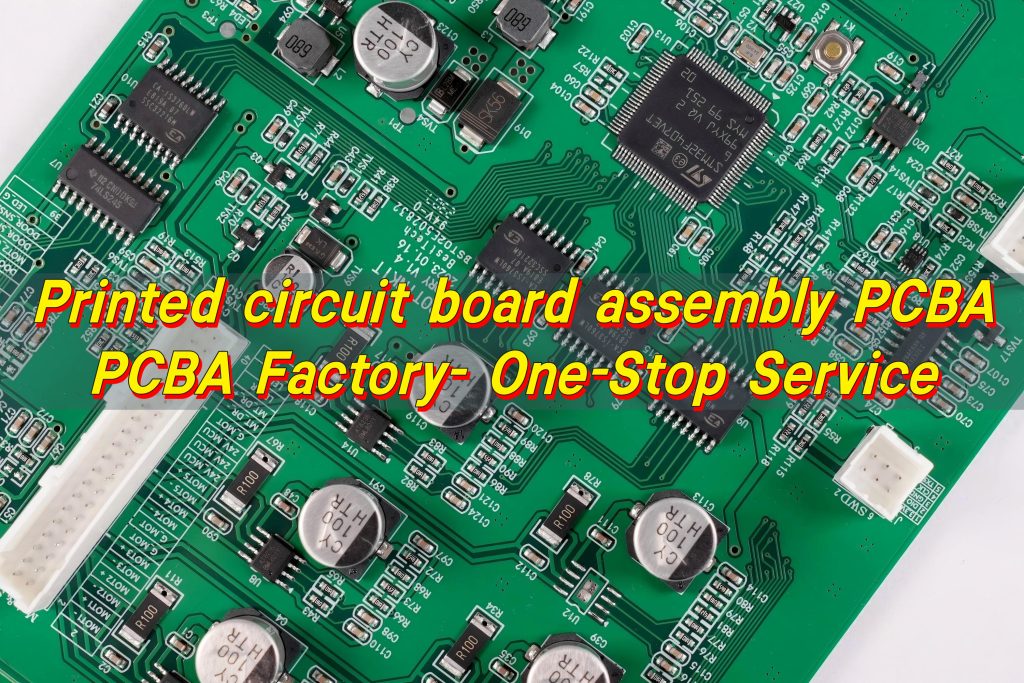
Printed Circuit Board Assembly PCBA, PCBA Factory – One-Stop Service
Printed circuit board assembly PCBA is the point where electronic design becomes a working product. Schematics turn into signals. Layouts turn into function. For engineers, PCBA is not just a manufacturing step. It is where performance, reliability, and cost finally meet reality.
As electronics become smaller and more integrated, printed circuit assembly demands tighter control, clearer processes, and deeper engineering awareness. From component sourcing to solder joint quality, every decision affects yield, lifetime, and field performance.
What is PCBA printed circuit board assembly?
PCBA meaning is simple in theory. It refers to a printed circuit board after all electronic components have been mounted and soldered. Before assembly, the board is only copper, laminate, and surface finish. After PCBA, it becomes a functional electronic unit.
Printed circuit board assembly PCBA includes much more than placing parts. It covers component preparation, soldering method selection, inspection, testing, and traceability. Each step must align with the board design and the electrical function.
There are two main ideas behind PCBA. The first is electrical connection. Signals must travel as designed. The second is mechanical stability. Components must survive vibration, heat, and time. PCBA brings these two requirements together in a controlled process.
Unlike bare PCB fabrication, PCBA errors are harder to fix. Rework risks damage. Scrap costs are higher. That is why assembly planning must start early.
What’s the difference between PCB and PCBA?
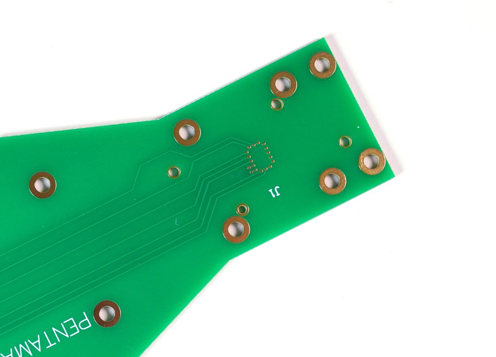
PCB vs PCBA is a common question. The difference is clear but important. A PCB is the physical board. It includes laminate, copper layers, solder mask, and surface finish. It has no electronic function by itself.
PCBA is the assembled version of that board. It includes resistors, capacitors, ICs, connectors, and other devices. Once assembled, the board can power on and perform tasks.
This difference matters in cost planning. PCB cost depends on layers, material, and fabrication complexity. PCBA cost depends on component count, package type, assembly method, and testing level.
In practice, PCB and PCBA must be treated as one system. Layout decisions affect assembly yield. Assembly constraints affect layout freedom. Treating them separately increases risk.
How is a PCB made step by step?
- The PCB process starts with material selection. FR-4 is common, but high-speed or high-temperature designs may use advanced laminates. Material choice affects signal loss, heat behavior, and assembly stability.
- Next comes inner layer imaging. Copper foils are patterned using photoresist and etching. These layers define signal routing and planes.
- Lamination follows. Inner layers are stacked with prepreg and pressed under heat and pressure. Poor lamination can lead to warpage, which later affects assembly quality.
- Drilling is next. Holes are created for vias and component leads. After drilling, holes are plated with copper to create electrical connections between layers.
- Outer layer imaging then defines surface traces and pads. Solder mask is applied to protect copper and control solder flow. Finally, surface finish such as ENIG or HASL is added to prepare for assembly.
Each step affects PCBA performance. For example, pad size and finish directly influence solder joint quality.
How many types of PCBA are there?
There are several ways to classify PCBA types. One common method is by assembly technology. Surface mount assembly places components directly onto pads. Through-hole assembly inserts leads into drilled holes. Many modern products use mixed assembly.
PCBA can also be classified by application requirement. Consumer electronics assembly focuses on cost and speed. Industrial and medical PCBA focus on reliability and traceability. Automotive PCBA adds thermal and vibration demands.
Each PCBA type requires different process controls. Fine-pitch BGA assembly needs precise stencil and reflow profiles. Power assemblies need strong solder fillets and thermal paths.
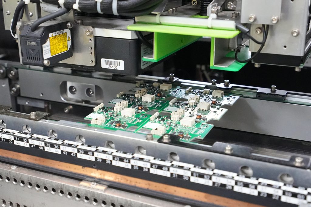
What is the PCB assembly process?
- The printed circuit board assembly process begins with preparation. Bare boards are inspected. Components are checked and sorted. Moisture-sensitive parts are baked if needed.
- Solder paste printing follows. A stencil deposits paste onto pads. Paste volume must match pad design. Too much causes bridges. Too little causes weak joints.
- Component placement comes next. Pick-and-place machines position parts with high accuracy. Orientation matters, especially for polarized devices.
- Reflow soldering then melts the paste. Temperature profiles must match solder alloy and component limits. Proper reflow creates strong, reliable joints. Poor profiles cause voids or cracks.
- For through-hole parts, wave or selective soldering is used. These processes require careful masking and temperature control.
- Inspection follows assembly. Optical inspection checks alignment and solder quality. X-ray inspection verifies hidden joints.
Each step connects to the next. Skipping control at any stage increases defect risk.
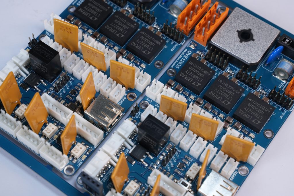
What are the components of a PCBA?
Printed circuit board assembly is made up of several functional element groups, each contributing to electrical performance and mechanical reliability:
- Passive components: Such as resistors, capacitors, and inductors, which control signal levels, timing, filtering, and power stability.
- Active components: Including ICs, microcontrollers, processors, and power management devices that handle logic, control, computation, and regulation.
- Interconnection components: Such as connectors, headers, sockets, and terminals that enable power input, signal transfer, and system integration.
- Sensing and interface devices: Sensors convert physical signals into electrical data, while interface components manage communication with external systems.
- The printed circuit board itself: The PCB substrate, copper layers, pad design, copper thickness, and surface finish all directly affect signal integrity and solder joint quality.
- Solder joints and attachment materials: Solder forms the electrical and mechanical bond between components and the board, defining long-term reliability.
- Supporting materials and markings: Solder paste alloy, flux chemistry, labels, conformal coatings, and identification marks support assembly quality, cleanliness, and traceability.
Because all these elements interact, PCBA must be treated as a complete system. At Best Technology, component selection, PCB fabrication, and assembly are coordinated under one workflow, reducing variation and protecting design intent.
What are the problems with PCBA?
Most PCBA issues originate from misalignment between design intent and manufacturing reality. Common challenges include:
- Design-to-process mismatch: Footprints, pad sizes, or spacing may not align with assembly capabilities or soldering methods.
- Soldering defects: Issues such as solder bridging, insufficient wetting, cold joints, and tombstoning often result from pad geometry or paste volume imbalance.
- Hidden joint reliability risks: BGA voiding and incomplete solder collapse can reduce long-term reliability if not properly controlled.
- Component availability and substitution risks: Alternate parts may differ in package, thermal mass, or solderability, introducing new assembly variables without engineering review.
- Board warpage during reflow: Thin boards, uneven copper distribution, or improper stack-ups can cause distortion, stressing solder joints and lowering yield.
While these problems are common, they are largely preventable. Best Technology addresses this early through DFM reviews before production begins.
What is a PCBA used for?
Printed circuit board assemblies are the functional core of nearly all electronic systems, across a wide range of industries:
- Consumer electronics: Compact PCBA designs enable smaller form factors, cost control, and high-volume production.
- Industrial equipment: Robust assemblies support long operating life, stable performance, and resistance to harsh environments.
- Medical devices: PCBA reliability directly affects patient safety, making process control and traceability critical.
- Automotive electronics: Assemblies must tolerate vibration, temperature extremes, and long service cycles.
- Communication and networking systems: Signal integrity, impedance control, and assembly consistency are essential for stable data transmission.
Best Technology supports PCBA across these application areas by offering turnkey PCB assembly services without MOQ requirements, allowing engineers to move from prototype to production using the same technical standards.
BEST Technology PCBA Services: PCB、Component、PCBA
BEST Technology delivers end-to-end printed circuit board assembly PCBA services designed around real engineering workflows, not fragmented supply chains. Instead of treating PCB fabrication, component sourcing, and assembly as separate tasks, we integrate them into a single, controlled manufacturing system.
Component sourcing is fully managed as part of our turnkey PCBA factory model. When shortages occur, our engineering team evaluates alternates based on electrical behavior, package compatibility, and assembly impact.
Printed circuit board assembly PCBA execution is controlled through disciplined processes. We support SMT, through-hole, and mixed-technology assembly under the same quality system. Fine-pitch ICs, BGAs, QFNs, and power devices are assembled using optimized stencil design, placement accuracy control, and tailored reflow profiles.
A critical advantage of Best Technology is flexibility without compromise. We offer turnkey PCB assembly service with no MOQ requirement, allowing engineers to prototype, validate, and scale using the same supplier, the same processes, and the same technical support team.
Conclusion:
Printed circuit board assembly PCBA is where design becomes reality. It combines structure, components, and process into a working system.
BEST Technology provides turnkey PCB assembly service without MOQ requirement, supporting engineers from early builds to stable production. Clear processes and engineering focus make the difference.
For project discussion or technical support, contact sales@bestpcb.vn