 language
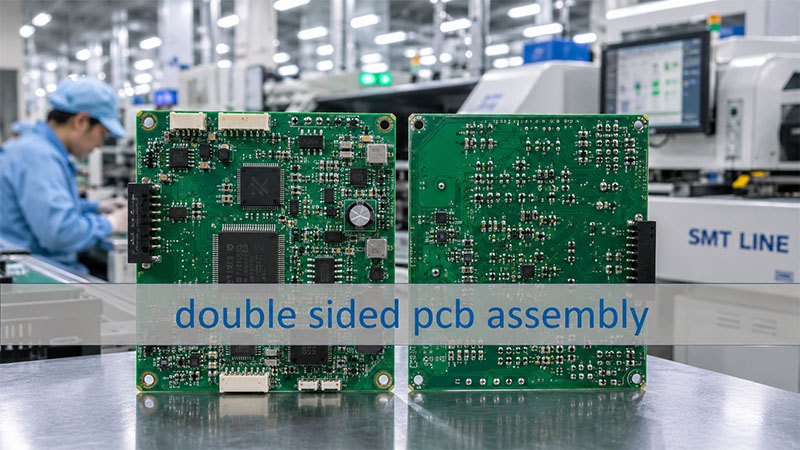
Double Sided PCB Assembly: Process, Design Rules, and Manufacturer Guide
Double sided PCB assembly means mounting electronic components on both sides of a printed circuit board, allowing engineers to fit more functions into a compact board size while improving layout flexibility. This article explains the process, key design rules, DFM considerations, and supplier selection points that help make double sided PCB assembly more reliable and production-ready.
Best Technology supports customers from PCB design and engineering review to PCB fabrication, component sourcing, PCBA assembly, and testing. With practical experience in RF, HDI, high-density layouts, and mixed assembly projects, our team helps customers reduce design risks before production starts. For support with your next double sided PCB assembly project, you can send your Gerber files, BOM, or design requirements to sales@bestpcb.vn.
What Is Double Sided PCB Assembly?
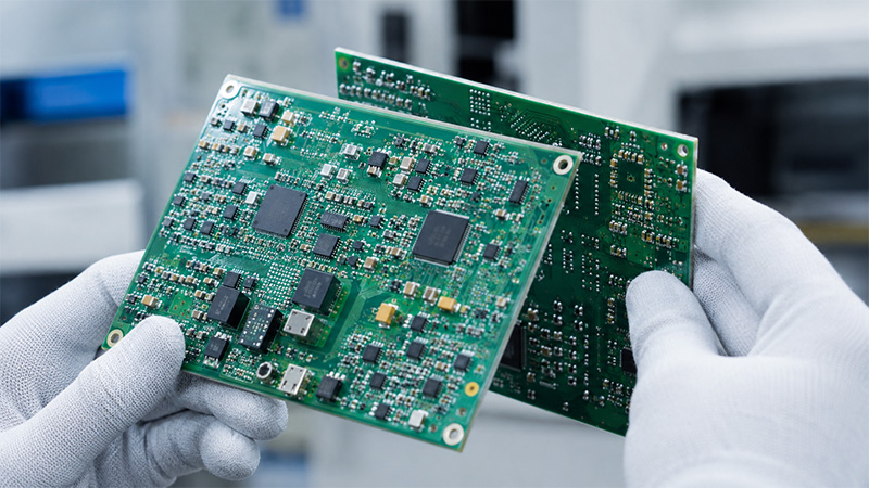
Double sided PCB assembly means placing electronic components on both the top and bottom sides of a printed circuit board. This method helps engineers use board space better. It also supports more functions in a smaller product size.
In many electronic products, one PCB side cannot hold all required parts. A compact control board may need ICs, connectors, resistors, capacitors, sensors, and power parts in a limited area. Therefore, engineers often use both PCB surfaces to create a more practical layout.
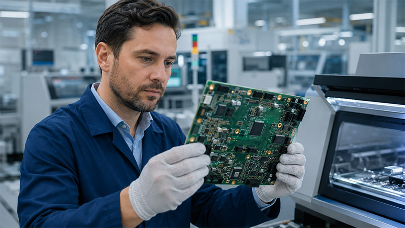
However, double sided assembly does not simply mean “put parts on two sides.” It needs careful PCB design, clear assembly planning, and strong process control. The board must support SMT placement, reflow soldering, inspection, testing, and final use.
Why Double Sided Assembly Matters
A good double sided PCB layout can reduce board size and shorten signal paths. It can also help engineers place connectors, chips, and power parts in better positions.
At the same time, poor planning can create issues. For example, heavy parts may move during the second reflow process. Dense placement may block AOI inspection. Missing test points may slow down troubleshooting. In addition, weak layout planning may increase heat, noise, or EMI risk.
For this reason, a reliable project should start with PCB design review, DFM checking, and process discussion. When design and assembly teams work together early, the final PCBA becomes easier to build and more stable in real use.
When Should You Use Double Sided PCB Assembly Instead of Single Sided Assembly?
You should use double sided PCB assembly when your product needs more components, a smaller board size, or better circuit organization than a single-sided layout can provide.
A single-sided PCB still works well for simple electronics. For example, basic LED boards, low-cost control panels, simple power boards, and basic consumer devices may not need two-sided component placement.
However, many modern products need more functions in less space. So, engineers use double sided assembly to improve layout flexibility.
Common Reasons to Choose Double Sided Assembly
You may need double sided PCBA when your design includes:
- Many ICs and passive components
- Limited product enclosure space
- Several connectors or interface ports
- Power circuits and signal circuits on one board
- High-speed or high-density routing
- Mixed SMT and through-hole components
- Compact industrial, medical, or communication modules
Also, double sided layout helps when the mechanical structure limits connector direction. For example, one connector may need to face the enclosure wall, while another interface may need to face the opposite side. In this case, one-sided placement may not work well.
Why Early Planning Helps
The best time to choose double sided assembly is during PCB design. If the team changes from single-sided to double-sided layout too late, the project may need extra redesign work.
Therefore, the design team should review the enclosure, component count, circuit density, thermal needs, and production method before layout starts. This early step can reduce design loops and improve production readiness.
What Is the Double Sided PCB Assembly Process?
The double sided PCB assembly process includes file review, PCB fabrication, SMT assembly on both sides, inspection, testing, and final quality control. The exact flow depends on board design and component types.
Main Process Flow
| Step | Process | Purpose |
|---|---|---|
| 1 | Schematic and PCB layout review | Check design risks before production |
| 2 | BOM and Gerber review | Confirm parts, footprints, polarity, and files |
| 3 | DFM and DFA review | Improve manufacturability and assembly flow |
| 4 | PCB fabrication | Produce bare boards according to design files |
| 5 | SMT stencil preparation | Prepare solder paste printing |
| 6 | First-side SMT assembly | Place and solder components on one side |
| 7 | Second-side SMT assembly | Place and solder components on the other side |
| 8 | THT or DIP assembly | Add through-hole parts when needed |
| 9 | AOI, X-ray, and functional test | Check solder joints and product performance |
| 10 | Final inspection and packing | Confirm quality before shipment |
Why the Soldering Sequence Matters
Double sided assembly needs a clear soldering sequence. Usually, the factory assembles one side first. Then, the team turns the board over and assembles the second side.
During the second reflow cycle, the first side goes through heat again. Therefore, the process engineer must review component weight, solder joint strength, pad design, and reflow profile.
Small resistors and capacitors usually stay stable during the second reflow process. Large inductors, heavy connectors, transformers, or tall capacitors need more attention. In some cases, the factory may use selective soldering, wave soldering, adhesive, or manual soldering for specific parts.
Because of this, the layout should match the real assembly process. A clean design can make production smoother and reduce assembly risk.
What Is the Difference Between Double Sided SMT and Mixed PCB Assembly?
Double sided SMT assembly and mixed PCB assembly often appear together, but they do not mean the same thing.
Double sided SMT assembly means the factory places surface-mount components on both sides of the PCB. Mixed PCB assembly means the board uses both SMT components and through-hole components.
Double Sided SMT Assembly
In double sided SMT assembly, most parts use surface-mount packages. These parts may include:
- Chip resistors
- MLCC capacitors
- ICs
- QFN packages
- BGA packages
- Diodes
- MOSFETs
- Sensors
- Small connectors
This method works well for compact and high-density electronics. It also supports fast automated placement.
Double Sided Mixed PCB Assembly
In mixed assembly, the board includes both SMT and THT parts. Through-hole parts often provide stronger mechanical support or higher current capability.
Common THT parts include:
- Terminal blocks
- Pin headers
- Relays
- Transformers
- Power inductors
- Large electrolytic capacitors
- High-current connectors
As a result, double sided mixed PCB assembly services often fit industrial control boards, inverter boards, power electronics, communication modules, and interface boards.
Simple Comparison
| Type | Main Feature | Suitable Products |
|---|---|---|
| Double sided SMT assembly | SMT parts on both sides | Compact control boards, communication boards, modules |
| Mixed PCB assembly | SMT and THT parts on one board | Industrial boards, power boards, interface boards |
| Double sided mixed assembly | SMT/THT parts across both sides | Dense boards with power, signal, and mechanical needs |
Therefore, the assembly type should guide the PCB layout. If the team ignores soldering, inspection, or connector direction, the board may become harder to build.
What PCB Design Rules Matter Most for Double Sided PCB Assembly?
PCB design strongly affects double sided PCB assembly quality. A good layout helps the factory place, solder, inspect, and test the board with fewer risks.
Component Placement on Both Sides
The design team should place components according to height, weight, heat sensitivity, signal function, and assembly sequence. This rule matters more in double sided assembly because both surfaces go through production steps.
Small passive parts often fit well on the bottom side. However, heavy or tall parts need extra care. These parts may include large capacitors, connectors, inductors, transformers, or mechanical parts.
In addition, the layout should leave enough space between components. Good spacing helps the SMT machine place parts accurately. It also helps AOI systems inspect solder joints more clearly.
SMT and Reflow Compatibility
The board must survive two reflow cycles. First, the factory solders one side. Next, it solders the second side. During the second cycle, the first side heats up again.
Therefore, the engineer should check whether the first-side components can remain stable. Pad size, solder paste volume, component weight, and reflow temperature all matter.
If the layout creates too much risk, the factory may adjust the process. However, layout optimization usually gives a better result than process repair.
Routing Density and Layer Planning
Double sided assembly often supports dense circuit designs. Because of that, routing strategy becomes very important.
The designer should plan power paths, signal routes, ground return paths, and thermal areas early. For RF, HDI, and high-speed boards, the design may also need controlled impedance, microvias, blind vias, or fine-line routing.
Good layer planning can improve signal quality and reduce noise. It can also make PCB fabrication and assembly more predictable.
Test Points and Inspection Access
The layout should give the test team enough access. Test points help engineers check power rails, signals, programming ports, and key circuit nodes.
Also, AOI machines need a clear view of solder joints. If components sit too close together, inspection becomes harder. For BGA, QFN, LGA, and other hidden-joint packages, X-ray inspection may also become necessary.
Panelization and Fiducial Marks
Panel design affects SMT efficiency. The PCB should include proper fiducial marks, tooling holes, board edge clearance, and panel support.
These details look small, but they can influence placement accuracy. Therefore, a DFM review should check them before production.
How Do DFM, SI, PI, and EMC Reviews Improve Double Sided PCB Assembly Quality?
DFM, SI, PI, and EMC reviews help the engineering team find risks before production. These reviews bring high value to double sided PCB assembly because dense boards leave less room for error.
DFM and DFA Review
DFM means Design for Manufacturability. It checks whether the PCB can move through fabrication and assembly smoothly.
DFA means Design for Assembly. It focuses on component placement, soldering sequence, inspection access, and production efficiency.
A strong DFM and DFA review may check:
- Pad size and footprint accuracy
- Solder mask clearance
- Component spacing
- Via design
- Copper balance
- Board thickness
- Surface finish
- Panelization
- Fiducial marks
- Test point access
- Bottom-side component risk
As a result, the team can fix many problems before SMT starts. This saves time and reduces rework.
SI Analysis
SI means Signal Integrity. It helps engineers check signal quality in high-speed circuits.
For example, SI review can help reduce reflection, crosstalk, impedance mismatch, and signal loss. This matters for boards with PCIe, Ethernet, DDR, RF circuits, optical communication, or fast digital signals.
If the product has high-speed signals, the design team should not wait until testing to solve these issues. Instead, they should review routing, impedance, return paths, and spacing during PCB layout.
PI Analysis
PI means Power Integrity. It checks whether each component receives stable power.
This review helps the team study voltage drop, power noise, decoupling capacitor placement, and power distribution paths. It matters for boards with processors, FPGAs, communication chips, high-current devices, or multiple power rails.
Good PI planning can reduce unstable startup, random reset, overheating, and noise issues.
EMC Review
EMC review focuses on electromagnetic compatibility. It helps reduce unwanted emissions and improve resistance to external interference.
For industrial, medical, automotive, and communication products, EMC performance can affect certification and market entry. Therefore, the design team should consider grounding, shielding, filtering, cable interfaces, return paths, and connector placement early.
Best Technology supports PCB design, DFM guidance, SI/PI-related review, EMC design consideration, PCB fabrication, component sourcing, PCBA assembly, and testing. This workflow helps customers move from schematic to final build with fewer design loops and better production control.
What Applications Commonly Use Double Sided PCB Assembly?
Double sided PCB assembly appears in many products that need compact size, stable performance, and practical production cost.
Industrial Control Electronics
Industrial control boards often include power circuits, signal circuits, connectors, sensors, and communication interfaces. These boards need stable performance in demanding working environments.
Double sided assembly helps engineers place more functions in a smaller space. It also supports mixed SMT and through-hole layouts.
Communication Equipment
Communication products often need dense component placement and clean signal routing. Examples include network modules, RF boards, optical communication boards, and data transmission devices.
In these products, layout quality can affect signal performance. Therefore, the design team should consider impedance, grounding, shielding, and return paths early.
Power and Inverter Electronics
Power products may include control ICs, drivers, relays, connectors, inductors, and high-current paths. Double sided mixed assembly can help separate control circuits from power sections.
This approach often works well for UPS control boards, inverter boards, battery management modules, and energy control devices.
Medical, Automotive, and Smart Devices
Medical electronics, automotive modules, robotics boards, and smart instruments often need compact and reliable PCBAs. Many of these products also require strict testing and clear traceability.
Therefore, early design review and reliable assembly control can improve product quality.
How to Choose a Reliable Double Sided PCB Assembly Manufacturer?
A reliable double sided PCB assembly manufacturer should offer more than basic SMT placement. The right partner should understand PCB design, DFM review, component sourcing, testing, and production control.
Check Engineering Support
First, review the supplier’s engineering ability. A good manufacturer can check Gerber files, BOM, pick-and-place files, assembly drawings, stackup, and component footprints.
If your project still needs design support, choose a supplier that can help with schematic review, PCB layout, stackup design, and DFM guidance.
Review Assembly Capability
Next, check whether the supplier can handle both SMT and THT assembly. Many double sided boards include connectors, relays, terminals, transformers, or large capacitors.
The supplier should understand soldering sequence, reflow control, selective soldering, AOI inspection, and X-ray inspection.
Confirm Testing and Quality Control
Testing matters in every PCBA project. The supplier should support suitable inspection and test methods based on product needs.
Useful methods include:
- AOI inspection
- X-ray inspection
- ICT
- Functional testing
- Visual inspection
- Final quality control
Also, clear quality records help customers track issues and improve future production.
Look for One-Stop Support
A one-stop partner can reduce project communication gaps. For example, Best Technology supports PCB design, PCB fabrication, component sourcing, PCBA assembly, testing, and final build.
This model works well for customers who want one engineering team to support the project from layout to production. It also helps when the product includes RF circuits, HDI structures, high-density layouts, industrial control boards, communication modules, or mixed assembly needs.
Need help reviewing your double sided PCB design before assembly? Send your Gerber files, BOM, or project requirements to sales@bestpcb.vn. Best Technology can help check your design files, review DFM risks, and suggest a practical path before production starts.
In a nutshell, double sided PCB assembly helps engineers build compact and functional electronic products. It supports higher component density, better layout flexibility, and more efficient product design.
However, successful assembly starts before SMT production. The project needs good PCB design, clear files, DFM review, suitable soldering sequence, reliable component sourcing, and proper testing.
Best Technology provides PCB design, engineering consultation, DFM guidance, PCB fabrication, component sourcing, PCBA assembly, testing, and production-quality support. With early collaboration, your double sided PCB project can move from prototype to manufacturing with better control and fewer risks.
If you need support for a new double sided PCB assembly project, send your Gerber files, BOM, or design requirements to sales@bestpcb.vn. Best Technology will help review your project and suggest a practical path from design to final build.
FAQs About Double Sided PCB Assembly
1. What files do I need for double sided PCB assembly?
You usually need Gerber files, BOM, pick-and-place files, assembly drawings, PCB specifications, and testing requirements. If the design needs review, schematic and layout files can also help.
2. Does double sided PCB assembly cost more than single-sided assembly?
Yes, it usually costs more because the board needs assembly on both sides. However, it can reduce PCB size and improve product integration. In some projects, this can lower the total product cost.
3. Can double sided PCB assembly support SMT and through-hole parts?
Yes. Many double sided PCBAs use both SMT and THT parts. This structure works well for industrial control boards, power electronics, communication equipment, and interface modules.
4. Do double sided PCBs need special design rules?
Yes. The design should consider component placement, soldering sequence, bottom-side part weight, test points, fiducials, panelization, and inspection access.
5. Can Best Technology help if my PCB design is not ready for assembly?
Yes. Best Technology can support schematic review, PCB layout, DFM guidance, stackup design, SI/PI-related review, EMC design advice, and manufacturing file preparation. This helps customers prepare their designs for smoother PCB fabrication and assembly.
6. Can double sided assembly work for RF, HDI, or high-speed boards?
Yes, but these boards need careful layout planning. The design team should review impedance, grounding, return paths, differential pairs, shielding, and routing density before production.
7. How long does double sided PCB assembly take?
Lead time depends on PCB complexity, component availability, quantity, testing needs, and whether the project includes PCB fabrication. Complete files and a clear BOM can help shorten the schedule.
8. How can I reduce production risk before assembly?
Start with engineering review. Check the schematic, PCB layout, DFM, DFA, BOM, component footprints, soldering sequence, test points, and inspection requirements before production starts.