 language
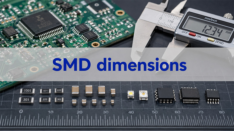
SMD Dimensions: Complete Size Reference for Resistors, Capacitors, LEDs & IC Packages
SMD dimensions are one of the most-referenced data points in PCB design. Whether you are selecting components for a new layout, checking footprint compatibility, or preparing files for PCBA assembly, knowing the exact size of each SMD package avoids costly mistakes downstream.
This guide covers everything in one place. You will find size charts for resistors, capacitors, LEDs, and IC packages — all with both metric (mm) and imperial (inch) values. We also explain what SMD and SMT mean, how to read package codes, and which sizes are easiest to assemble in production.
Best Technology is a professional one-stop PCBA manufacturer based in Vietnam. We have served over 10,000 engineers and 1,800 customers across 20 years of PCB and PCBA manufacturing. We work with all standard SMD package sizes — from 01005 to large through-hole packages — and we understand the assembly implications of each one. If you are planning a new PCBA project, we would be glad to help you get it right from the start.
What Is SMD? SMD vs SMT Explained
SMD stands for Surface Mount Device. It refers to any electronic component that mounts directly onto the surface of a PCB. The component sits on pads rather than being inserted through drilled holes. This is how the vast majority of modern electronic components are packaged and assembled.
SMT stands for Surface Mount Technology. It is the broader term for the entire assembly process — the equipment, solder paste printing, pick-and-place machines, reflow ovens, and inspection steps that are used to attach SMDs to a board. In short, SMD is the component type. SMT is the process.
These two terms are often used interchangeably in practice. However, it is more accurate to say that SMT assembles SMDs. When someone asks about SMD dimensions, they are almost always asking about component body sizes and their corresponding PCB footprints.
Before SMD packaging became standard, most components used through-hole technology (THT). Through-hole parts had long leads that went through drilled holes and were soldered on the back of the board. SMD components eliminated those leads. As a result, they are smaller, lighter, and much better suited for high-density layouts and automated assembly.
How to Read SMD Package Codes?
SMD package codes look like numbers — 0402, 0603, 0805, 1206 — and many engineers use them without knowing exactly what they mean. In fact, the code is a direct description of the component’s dimensions.
The code uses the imperial (inch) system. Each digit pair represents a dimension in hundredths of an inch. So 0402 means the component body is 0.04 inches long and 0.02 inches wide. That converts to 1.0 × 0.5 mm in metric.
There is an important naming difference to be aware of. The standard EIA code uses imperial units — so 0402 means 1.0 × 0.5 mm. However, the IEC metric equivalent for the same physical size is 1005. This can cause confusion. When reading a datasheet or ordering components, always check whether the size code is imperial (EIA) or metric (IEC).
Quick rule: if the package code has four digits and the first two are 04 or larger, it is likely an imperial EIA code. If the first two digits are 10 or larger (like 1005 or 1608), it may be an IEC metric code for the same or similar physical size.
Standard SMD Dimensions: Full Size Chart
The table below lists all commonly used SMD package sizes, from the smallest to the largest. Both imperial (EIA) and metric (IEC) codes are shown, along with the physical body dimensions.
| EIA Code (Imperial) | IEC Code (Metric) | Length (mm) | Width (mm) | Typical Use |
|---|---|---|---|---|
| 01005 | 0402 | 0.4 | 0.2 | Advanced mobile, wearables |
| 0201 | 0603 | 0.6 | 0.3 | Mobile phones, compact PCBs |
| 0402 | 1005 | 1.0 | 0.5 | Consumer electronics, IoT |
| 0603 | 1608 | 1.6 | 0.8 | General electronics, most popular |
| 0805 | 2012 | 2.0 | 1.25 | Industrial, power, general use |
| 1206 | 3216 | 3.2 | 1.6 | Higher power, precision resistors |
| 1210 | 3225 | 3.2 | 2.5 | High-capacitance capacitors |
| 1812 | 4532 | 4.5 | 3.2 | High-voltage capacitors, fuses |
| 2010 | 5025 | 5.0 | 2.5 | High-power resistors |
| 2512 | 6332 | 6.3 | 3.2 | Current sense resistors, high power |
The most commonly used sizes in general electronics are 0402, 0603, and 0805. These three cover the majority of consumer, industrial, and IoT designs. Sizes below 0402 (such as 0201 and 01005) require advanced assembly processes and are mainly found in high-density mobile or wearable products.
SMD Resistor Dimensions
SMD resistors are the most common surface mount component by volume. Almost every PCB contains dozens or hundreds of them. They follow the standard EIA package size system described above, so their dimensions match the full size chart directly.
However, there are a few additional dimensions that matter specifically for resistors. These affect both PCB footprint design and assembly process parameters.
| Package | Body L × W (mm) | Height (mm) | Pad Width (mm) | Pad Length (mm) |
|---|---|---|---|---|
| 0201 | 0.6 × 0.3 | 0.23 | 0.25 | 0.30 |
| 0402 | 1.0 × 0.5 | 0.35 | 0.50 | 0.50 |
| 0603 | 1.6 × 0.8 | 0.45 | 0.80 | 0.70 |
| 0805 | 2.0 × 1.25 | 0.50 | 1.20 | 0.80 |
| 1206 | 3.2 × 1.6 | 0.55 | 1.60 | 0.80 |
| 1210 | 3.2 × 2.5 | 0.55 | 2.50 | 0.80 |
| 2010 | 5.0 × 2.5 | 0.60 | 2.50 | 1.00 |
| 2512 | 6.3 × 3.2 | 0.60 | 3.20 | 1.00 |
The pad dimensions shown are typical recommended values for reflow soldering. They may vary slightly between component manufacturers and PCB design tools. In general, it is best to follow the pad dimensions in the component’s own datasheet rather than relying on generic values.
Assembly note: for 0402 resistors and smaller, stencil aperture design becomes critical. Insufficient paste volume causes tombstoning. Excess paste causes bridging. Both issues are common during first-article builds with these package sizes.
SMD Capacitor Dimensions
SMD capacitors share the same package codes as resistors. However, their physical dimensions can differ slightly from resistors in the same package. This is because capacitors — especially multilayer ceramic capacitors (MLCCs) — are often specified with tighter body thickness tolerances due to their internal layer structure.
The most common SMD capacitor packages and their dimensions are as follows:
| Package | Body L × W (mm) | Height (mm) | Common Capacitance Range |
|---|---|---|---|
| 0201 | 0.6 × 0.3 | 0.30 | 1 pF – 100 nF |
| 0402 | 1.0 × 0.5 | 0.50 | 0.5 pF – 10 µF |
| 0603 | 1.6 × 0.8 | 0.80 | 0.5 pF – 22 µF |
| 0805 | 2.0 × 1.25 | 1.25 | 0.5 pF – 47 µF |
| 1206 | 3.2 × 1.6 | 1.60 | 1 pF – 100 µF |
| 1210 | 3.2 × 2.5 | 2.50 | 100 pF – 100 µF |
| 1812 | 4.5 × 3.2 | 3.20 | 1 nF – 47 µF (high voltage) |
One important point about capacitor package selection: two capacitors in the same package size can behave very differently depending on dielectric type (X5R, X7R, C0G, Y5V) and voltage rating. These electrical properties affect component height as well. A high-capacitance 0805 capacitor with an X5R dielectric may be taller than a low-capacitance one. Always check the component datasheet for the actual height, especially in low-profile designs.
Electrolytic SMD Capacitors
Tantalum and aluminum electrolytic capacitors also come in SMD packages. However, they use different package codes — typically letter designations (A, B, C, D, E) for tantalum, and case codes like 4 × 5.4 mm or 6.3 × 5.4 mm for aluminum electrolytic. These are not interchangeable with the ceramic capacitor codes above.
SMD LED Dimensions
SMD LEDs follow the same package naming convention as resistors and capacitors for the smaller sizes. However, larger SMD LEDs — especially power LEDs — have their own package families with different naming systems.
Standard SMD LED Package Sizes
| Package | Body L × W (mm) | Height (mm) | Typical Application |
|---|---|---|---|
| 0402 | 1.0 × 0.5 | 0.35 | Indicator lights, backlighting |
| 0603 | 1.6 × 0.8 | 0.55 | Status indicators, keyboards |
| 0805 | 2.0 × 1.25 | 0.70 | General indicator use |
| 1206 | 3.2 × 1.6 | 1.10 | Higher brightness indicators |
Power SMD LED Packages
Power LEDs use different package codes. The most common ones are named by their dimensions in tenths of a millimeter. For example, the 2835 package measures 2.8 × 3.5 mm. The 5050 package measures 5.0 × 5.0 mm.
| Package | Body L × W (mm) | Height (mm) | Power Range |
|---|---|---|---|
| 2835 | 2.8 × 3.5 | 0.7 | 0.1 W – 1 W |
| 3528 | 3.5 × 2.8 | 1.9 | 0.1 W – 0.5 W |
| 5050 | 5.0 × 5.0 | 1.6 | 0.2 W – 0.5 W (RGB common) |
| 5630 / 5730 | 5.6 × 3.0 | 0.9 | 0.5 W – 1 W |
| COB (various) | varies | varies | 3 W – 100 W+ |
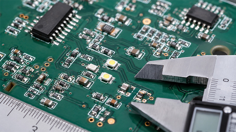
For PCB assembly, SMD LEDs introduce an additional challenge compared to resistors or capacitors. LEDs are sensitive to electrostatic discharge (ESD) and thermal stress. During reflow soldering, the temperature profile must stay within the LED manufacturer’s specified limits. Exceeding the peak temperature even briefly can permanently shift the color point or reduce lumen output.
SMD IC Package Dimensions and Types
ICs (integrated circuits) use a wider variety of SMD package types than passive components. Each package type has different dimensions, pin counts, pin spacing (pitch), and assembly requirements. Choosing the right package affects both PCB layout density and the assembly process needed.
Common SMD IC Package Types
| Package Type | Full Name | Pin Count Range | Typical Pitch |
|---|---|---|---|
| SOT-23 | Small Outline Transistor | 3 – 8 pins | 0.95 mm |
| SOT-223 | Small Outline Transistor (power) | 3 – 4 pins | 2.30 mm |
| SOIC / SO | Small Outline IC | 8 – 44 pins | 1.27 mm |
| SSOP | Shrink Small Outline Package | 8 – 56 pins | 0.65 mm |
| TSSOP | Thin Shrink Small Outline Package | 8 – 80 pins | 0.65 mm |
| QFP / LQFP | Quad Flat Package | 32 – 256 pins | 0.4 – 0.8 mm |
| QFN | Quad Flat No-Lead | 8 – 100 pins | 0.4 – 0.65 mm |
| BGA | Ball Grid Array | 36 – 1000+ pins | 0.4 – 1.27 mm |
| LGA | Land Grid Array | varies | 0.5 – 1.0 mm |
Key Dimensions for SMD IC Packages
Unlike passive SMD components, IC packages cannot be described by a single size code. Instead, their dimensions depend on the specific variant. For example, a SOIC-8 package measures 4.9 × 3.9 mm with a 1.27 mm pin pitch. A SOIC-16 in the wide body version measures 10.3 × 7.5 mm. Always refer to the component datasheet for the exact body size, lead span, and pad dimensions.
A few package families deserve special attention:
QFN packages have exposed thermal pads on the bottom. These require careful stencil design to avoid solder voiding underneath the IC. The thermal pad also needs a via pattern to conduct heat into the inner copper layers of the PCB.
BGA packages have solder balls arranged in a grid on the bottom. None of the connections are visible after assembly. This means X-ray inspection is required to verify solder joint quality. For this reason, BGA assembly demands tighter process control than leaded packages.
SOIC packages are among the easiest SMD ICs to assemble and rework. Their 1.27 mm pitch is wide enough for reliable soldering with standard SMT equipment, and individual pins can be reworked with a soldering iron if needed.
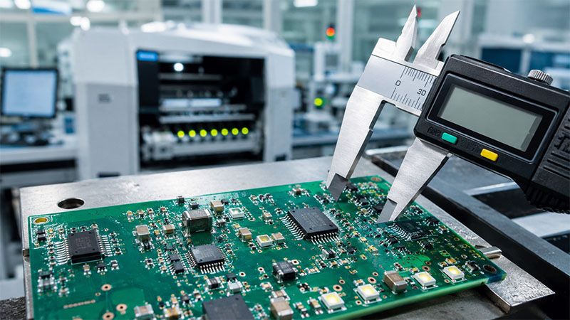
SMD Dimensions and Assembly Considerations
Knowing the physical dimensions of an SMD package is only part of the picture. The assembly process also depends on several factors that are directly linked to component size.
Stencil Aperture and Solder Paste Volume
Smaller components need smaller stencil apertures. The aperture aspect ratio — opening width divided by stencil thickness — must be greater than 1.5 for reliable paste release. For 0402 components, this typically means a stencil thickness of 0.12 mm or less. For 0201 and below, the stencil design becomes even more critical.
Pick-and-Place Accuracy
Modern pick-and-place machines place 0402 and 0603 components reliably at speeds of thousands of placements per hour. However, 0201 and 01005 components require machines with higher vision resolution and finer mechanical tolerance. Not every SMT line can handle these sizes — it is worth confirming capability before designing them into a layout.
Reflow Profile
Larger SMD packages have more thermal mass. As a result, they take longer to reach solder melting temperature during reflow. In mixed-component assemblies — where small 0402s and large QFPs are on the same board — the reflow profile must be designed to heat everything adequately without overheating the small components first.
Component Spacing and Clearance
SMD dimensions also affect minimum component spacing rules. The IPC-7351 standard provides recommended courtyard clearances for each package type. Following these rules prevents component shadow effects during reflow and allows adequate access for inspection and rework.
Assembly note: mixing very small SMD sizes (0201 or smaller) with large packages on the same side of the board increases process complexity significantly. Where possible, group components by size on each board side to simplify the assembly process.
How Best Technology Handles SMD Assembly in Vietnam?
At Best Technology, we are Vietnam’s professional one-stop PCBA service provider. We understand what engineers need — and we know that SMD package selection affects every stage of the manufacturing process, from DFM review to stencil design to final testing.
We have been manufacturing PCBs and PCBA for 20 years. In that time, we have assembled boards ranging from 01005-populated RF modules to large industrial control boards with 1000+ pin BGAs. Our team understands the assembly implications of every package size in this guide.
What We Offer for SMD Assembly Projects
Every order at Best Technology comes with a dedicated account manager and a three-person engineering team. Before production starts, we deliver a DFM report and a BOM optimization list. For SMD-dense designs, our DFM review covers stencil aperture ratios, component spacing, pad dimension checks against component datasheets, and thermal pad via recommendations for QFN and BGA packages.
Our SMD assembly capabilities include the following:
- SMT assembly supporting all standard package sizes from 01005 to large QFP and BGA
- BGA assembly with X-ray inspection for hidden joint verification
- QFN and thermal pad assembly with optimized stencil aperture design
- Through-hole assembly (THT) for mixed-technology boards
- Flex PCB assembly and ceramic PCB assembly for specialist applications
- Component sourcing from authorized distributors — all SMD sizes covered
- Prototype, small-batch, and volume production from one facility
- 1.5-week PCBA turnaround from Gerber files to shipped, tested boards
Our Certifications
We hold ISO 9001, ISO 13485, IATF 16949, and AS9100D. This means we are qualified for general commercial electronics, medical device assembly, automotive electronics, and aerospace applications. Our digital MES system tracks every material lot and batch — retrievable in under five seconds.
To get a quote or discuss your SMD assembly project, contact our engineering team at sales@vn.danyupcbs.com or call +84-827-237566. Send us your Gerber files and BOM, and we will return a DFM report and quote within 24 hours.
FAQs About SMD Dimensions
What does SMD stand for?
SMD stands for Surface Mount Device. It refers to any electronic component designed to sit on the surface of a PCB rather than pass through drilled holes. SMD is closely related to SMT (Surface Mount Technology), which is the assembly process used to solder SMDs onto the board. The two terms are often used interchangeably, but SMD describes the component and SMT describes the process.
What are standard SMD dimensions?
Standard SMD package codes are based on the EIA imperial system. The code directly describes the component’s size in hundredths of an inch. For example, 0402 is 0.04 × 0.02 inches, which equals 1.0 × 0.5 mm. Common sizes range from 01005 (0.4 × 0.2 mm) at the smallest end to 2512 (6.3 × 3.2 mm) at the larger end.
What is the difference between 0402 and 0603 SMD components?
Both are widely used, but they differ in size and assembly complexity. 0402 measures 1.0 × 0.5 mm and requires more precise paste printing and placement. 0603 measures 1.6 × 0.8 mm and is somewhat easier to handle. In practice, 0603 is the more forgiving choice for designs that do not require extreme miniaturization.
What SMD sizes are easiest to assemble?
0603 and 0805 offer the best balance of compact size and assembly reliability. They are small enough for high-density layouts but large enough for standard SMT equipment to handle without special processes. 0402 is also very common and well within the capability of modern SMT lines. Sizes below 0402 require specialized equipment and tighter process controls.
What is the smallest standard SMD package?
The smallest widely used package is 01005, measuring 0.4 × 0.2 mm. Assembling 01005 requires advanced pick-and-place machines, ultra-fine stencil apertures, and very tight process controls. It is mainly used in high-density mobile and wearable electronics where board space is extremely limited.
Do SMD resistors and capacitors in the same package size have the same dimensions?
Their body length and width are nominally the same, but height can differ. Capacitors — especially MLCCs at higher capacitance values — tend to be taller than resistors in the same package. Always check the component datasheet for the exact height, as this affects clearance in low-profile assemblies and conformal coating processes.
Can Best Technology assemble boards with very small SMD components?
Yes. We support all standard SMD sizes including 01005, 0201, and 0402. For fine-pitch BGA and QFN packages, we provide X-ray inspection and optimized stencil design as standard. Contact us at sales@vn.danyupcbs.com or +84-827-237566 to discuss your specific package requirements.