 language
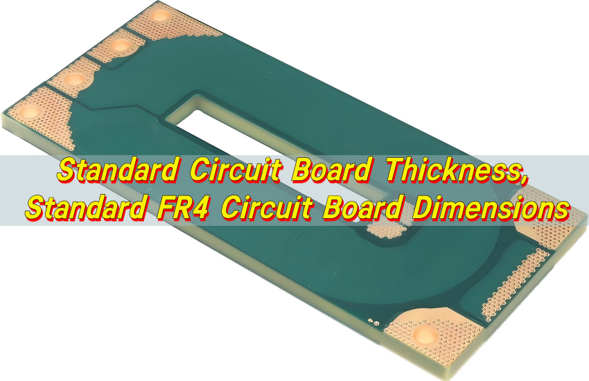
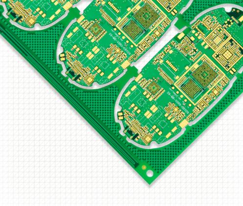
Standard Circuit Board Thickness, Standard FR4 Circuit Board Dimensions
Printed circuit boards sit at the heart of nearly every modern electronic product, yet their physical structure is often overlooked until a design challenge appears. Among the many design parameters, thickness plays a decisive role in performance, durability, manufacturability, and cost. Whether you are designing a compact wearable device or a high-power industrial controller, understanding standard circuit board thickness is essential to making confident engineering decisions.
In practical manufacturing environments, thickness is not just a number—it represents a balance between electrical integrity, mechanical stability, and production efficiency. Engineers who grasp this balance can avoid unnecessary redesigns, reduce costs, and improve product reliability.
How thick is a typical circuit board?
A typical printed circuit board thickness is 1.6 mm (0.063 inches). This value has become widely accepted across the electronics industry because it offers a reliable compromise between strength and usability. It is neither too fragile for handling nor too thick for standard connectors and enclosures.
However, calling 1.6 mm “standard” does not mean it is universal. PCB thickness varies depending on application, layer count, and mechanical requirements. In practice, commonly used thickness ranges include:
- 0.4 mm – 0.8 mm: Ultra-thin boards for compact or flexible applications
- 1.0 mm – 1.2 mm: Lightweight consumer electronics
- 1.6 mm: Industry default for general-purpose designs
- 2.0 mm – 3.2 mm: Heavy-duty or high-power applications
The popularity of 1.6 mm comes from decades of standardization across component manufacturers, enclosure designers, and assembly processes. Connectors, card slots, and mounting hardware are often designed with this thickness in mind, which simplifies integration.
At Best Technology, most global customers still prefer 1.6 mm boards for standard projects, especially in communication devices, industrial control systems, and consumer electronics. This consistency reduces production complexity and shortens lead times.
What is the best thickness for PCB?
There is no single “best” thickness for all PCB designs. Instead, the optimal thickness depends on the specific application and operating environment. Choosing the right thickness requires a clear understanding of electrical, mechanical, and thermal demands.
A thinner PCB may be ideal for compact devices, but it can introduce challenges such as warping or reduced mechanical strength. On the other hand, thicker boards offer durability but may increase cost and complicate high-density routing.
When selecting thickness, engineers typically evaluate:
- Mechanical strength: Thicker boards resist bending and vibration
- Weight constraints: Thinner boards reduce overall device weight
- Signal performance: Controlled impedance designs may require specific thickness
- Thermal management: Thicker boards can improve heat dissipation in some cases
- Assembly compatibility: Standard thickness simplifies SMT and connector fitting
For example, a wearable medical device benefits from a thin, lightweight PCB, while an industrial motor controller requires a thicker board to withstand harsh conditions.
A practical way to approach this decision is to align thickness with product category:
| Application Type | Recommended Thickness |
|---|---|
| Wearable electronics | 0.4 – 0.8 mm |
| Consumer devices | 1.0 – 1.6 mm |
| Industrial equipment | 1.6 – 2.4 mm |
| High-power systems | 2.0 – 3.2 mm |
Experienced manufacturers like Best Technology often guide customers through this selection process by evaluating both design intent and production feasibility. This collaborative approach ensures the final product meets both technical and commercial expectations.
What is the standard thickness and weight of a copper layer on a PCB?
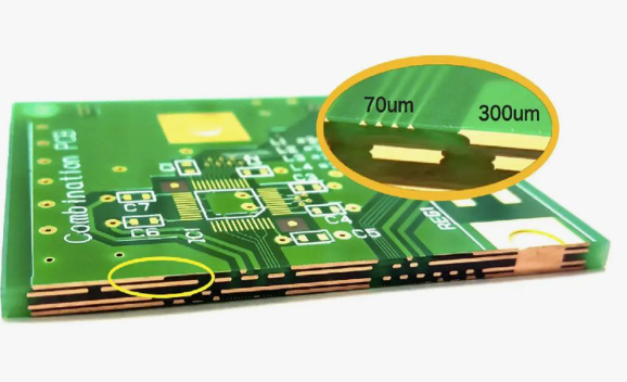
While overall board thickness is important, copper thickness directly affects electrical performance. Copper layers carry current, influence impedance, and contribute to heat dissipation. Therefore, understanding copper weight is essential for achieving stable circuit behavior.
Copper thickness is usually expressed in ounces per square foot (oz/ft²). The most common standard values are:
- 1 oz copper (≈ 35 µm) – Standard for most applications
- 0.5 oz copper (≈ 17 µm) – Fine-line, high-density circuits
- 2 oz copper (≈ 70 µm) – High-current designs
- 3 oz+ copper – Power electronics and heavy-duty applications
The relationship between copper weight and thickness is straightforward:
| Copper Weight | Approximate Thickness |
|---|---|
| 0.5 oz | 17 µm |
| 1 oz | 35 µm |
| 2 oz | 70 µm |
| 3 oz | 105 µm |
In most standard circuit board thickness configurations, 1 oz copper is the default choice because it provides sufficient conductivity without increasing cost significantly.
However, higher copper thickness is often required in:
- Power supply circuits
- Automotive electronics
- Industrial control systems
- LED lighting applications
Choosing the right copper thickness ensures efficient current flow while preventing overheating and voltage drop. It also impacts trace width design, which is critical for safety and performance.
Why are PCBs 1.6 mm thick?
The widespread adoption of 1.6 mm PCB thickness is not accidental. It reflects a historical convergence of mechanical, electrical, and manufacturing considerations that proved highly effective across multiple industries.
Several factors explain why 1.6 mm became the industry benchmark:
- Mechanical reliability: Provides sufficient rigidity for handling and assembly
- Compatibility: Matches standard connectors and card-edge designs
- Cost efficiency: Optimized material usage and manufacturing processes
- Thermal balance: Adequate heat dissipation without excessive bulk
- Global standardization: Widely supported by suppliers and equipment
In earlier stages of electronics manufacturing, different thicknesses were experimented with. Over time, 1.6 mm emerged as the most practical choice for mass production. It allowed manufacturers to streamline tooling, reduce variability, and improve yield rates.
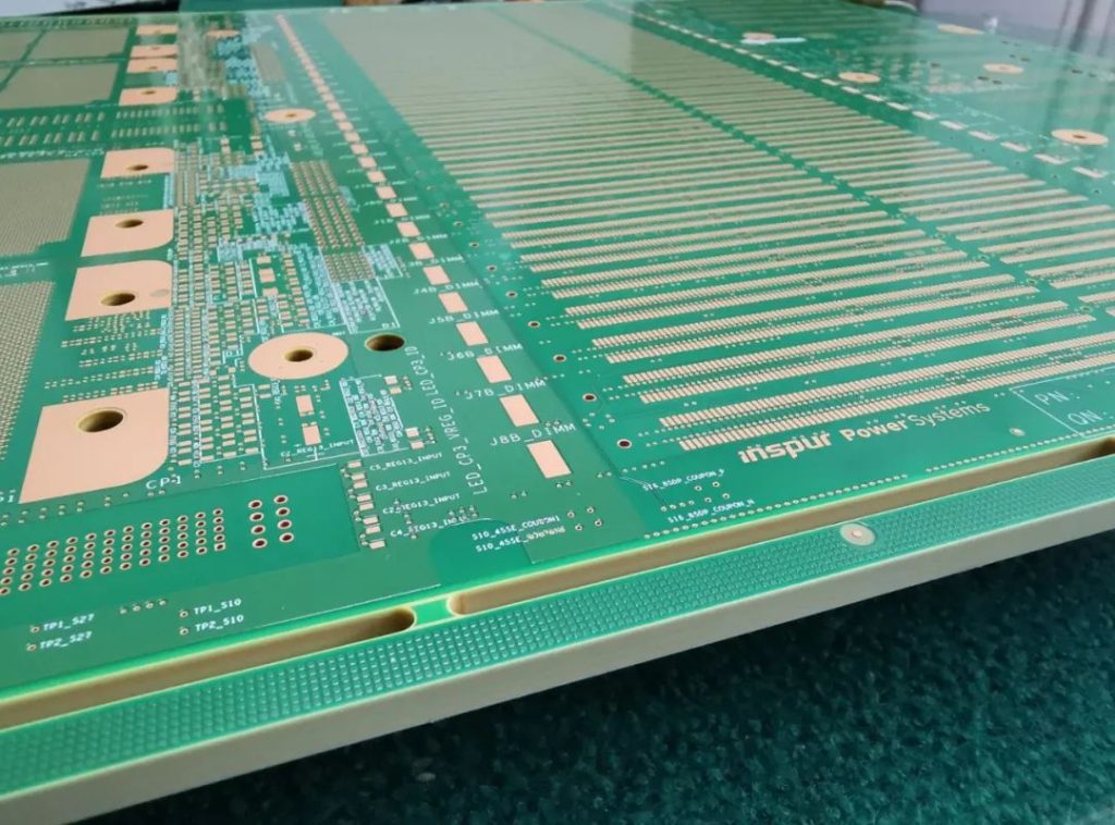
From a production standpoint, maintaining a standard thickness simplifies panelization, drilling, and lamination processes. It also reduces the risk of defects such as warping or delamination.
At Best Technology, maintaining strict control over thickness tolerance ensures consistent product quality. This is especially important in high-volume production, where even minor deviations can affect assembly performance.
How thick is a 4 layer PCB board?
A 4-layer PCB typically has a thickness ranging from 1.2 mm to 1.6 mm, with 1.6 mm being the most common standard. The final thickness depends on the stack-up design, which includes core material, prepreg layers, and copper thickness.
A standard 4-layer stack-up includes:
- Top signal layer
- Inner ground plane
- Inner power plane
- Bottom signal layer
The thickness distribution is influenced by dielectric spacing and copper weight. Engineers often adjust these parameters to achieve controlled impedance and signal integrity.
Here is a simplified comparison of 4-layer PCB thickness options:
| Configuration | Typical Thickness |
|---|---|
| Compact design | 1.2 mm |
| Standard design | 1.6 mm |
| High-power design | 2.0 mm+ |
A 4-layer PCB offers significant advantages over 2-layer designs, including improved signal routing, reduced electromagnetic interference, and better power distribution.
For high-speed applications such as communication modules or embedded systems, the ability to include dedicated ground and power planes makes 4-layer boards highly effective.
How thick is a 2 layer FR-4 PCB?
A 2-layer FR-4 PCB is one of the simplest and most widely used board types. Its thickness typically ranges from 0.8 mm to 1.6 mm, depending on the application.
FR-4 is the standard substrate material used in most PCBs. It is a glass-reinforced epoxy laminate known for its excellent electrical insulation, mechanical strength, and cost-effectiveness.
Common thickness options for 2-layer FR-4 boards include:
- 0.8 mm: Compact devices and lightweight designs
- 1.0 mm: Moderate strength with reduced weight
- 1.6 mm: Standard general-purpose thickness
Compared to multi-layer boards, 2-layer PCBs are easier to manufacture and more cost-efficient. However, they offer limited routing space and are less suitable for complex circuits.
A quick comparison highlights the differences:
| Feature | 2-Layer PCB | 4-Layer PCB |
|---|---|---|
| Complexity | Low | Moderate |
| Cost | Lower | Higher |
| Signal integrity | Basic | Improved |
| Routing flexibility | Limited | Enhanced |
| Thickness range | 0.8–1.6 mm | 1.2–1.6 mm |
For many consumer electronics and simple control systems, 2-layer FR-4 boards remain a practical and efficient choice.
How to know PCB thickness?
Determining PCB thickness can be done through several reliable methods, depending on the stage of the project. In the design phase, thickness is specified in the fabrication drawing or stack-up documentation. This ensures that manufacturers clearly understand the required structure.
During production or inspection, thickness can be measured using:
- Calipers or micrometers: Direct physical measurement
- Cross-section analysis: Detailed inspection of internal layers
- Manufacturer specifications: Datasheets and production reports
For engineers working with existing boards, measuring thickness accurately helps in reverse engineering or redesign projects.
It is also important to consider tolerance, which typically ranges from ±10% of the nominal thickness. Maintaining tight tolerance is crucial for applications involving connectors or precise mechanical assembly.
Best Technology provides detailed stack-up documentation and thickness verification reports to ensure transparency and accuracy throughout the production process.
What is the minimum PCB thickness?
The minimum PCB thickness depends on material limitations and manufacturing capabilities. In most cases, the practical minimum thickness for rigid PCBs is around 0.2 mm to 0.4 mm.
Ultra-thin PCBs are used in specialized applications such as:
- Wearable electronics
- Medical devices
- Flexible or semi-flexible circuits
- Compact IoT modules
However, reducing thickness introduces challenges, including:
- Increased risk of bending or warping
- Reduced mechanical durability
- Handling difficulty during assembly
While thinner boards offer clear advantages in terms of weight and space, they require careful design and precise manufacturing control. This is where experienced suppliers play a critical role in ensuring reliability.
Conclusion:
Standard circuit board thickness is more than just a specification—it is a key factor that influences performance, durability, and manufacturability. From the widely adopted 1.6 mm standard to specialized ultra-thin designs, each thickness option serves a distinct purpose.
Best Technology brings years of manufacturing expertise to support customers in choosing the most suitable PCB configurations. With strict quality control, fast response times, and flexible production capabilities, the company helps transform design concepts into reliable products.
For professional PCB solutions and technical support, feel free to reach out at sales@bestpcb.vn.