 language
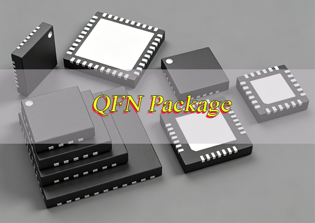
What is QFN Package? DFN VS QFN VS QFP Package
Are you searching for a clear understanding of QFN package technology and how it compares to other common IC packages? The QFN package stands as one of the most widely adopted surface mount packaging solutions in modern electronics, offering a unique blend of compact size, excellent thermal performance, and high electrical efficiency.
This guide breaks down every critical aspect of the QFN package, from its fundamental definition and internal structure to manufacturing processes, soldering techniques, cost factors, and detailed comparisons with DFN, QFP, LGA, and WLCSP packages. By exploring these elements, you will gain the technical knowledge needed to select the optimal package type for your PCB designs, ensuring enhanced performance, reliability, and manufacturability in both prototype and mass production environments.
What is QFN Packaging? What is its Full Form?
QFN package stands for Quad Flat No-leads package. It is a compact, surface mount integrated circuit (IC) packaging technology characterized by its square or rectangular form factor, absence of protruding external leads, and perimeter metallized contact pads located on the package bottom.
The QFN package typically features a large central exposed thermal pad (EPAD) that significantly enhances heat dissipation capabilities. This leadless design delivers a smaller footprint, lower profile, and shorter electrical paths compared to leaded packages, making it ideal for high-density PCB applications, portable electronics, and high-frequency circuits.
The QFN package is also known by alternative industry designations such as MLF (Micro Lead Frame), SON (Small Outline No-lead), and LPCC (Leadless Plastic Chip Carrier), all referring to the same core leadless quad flat package architecture.
What is the Thermal Resistance of the QFN package?
Thermal resistance measures a package’s ability to dissipate heat, with lower values indicating superior thermal performance. The QFN package delivers exceptional thermal characteristics primarily through its central exposed thermal pad. Typical thermal resistance values for a standard QFN package include θJA (junction-to-ambient) ranging from 20°C/W to 45°C/W, θJC (junction-to-case) between 0.5°C/W and 2°C/W, and θJB (junction-to-board) from 1°C/W to 3°C/W. These values vary based on package size, pin count, thermal pad dimensions, PCB copper coverage, and thermal via implementation. When properly designed with thermal vias under the central pad, the QFN package achieves thermal resistance up to 50% lower than comparable QFP packages, enabling effective heat dissipation for high-power ICs in compact spaces.
QFN Package Datasheet
| Parameter | Specification Details |
|---|---|
| Full Form | Quad Flat No-leads |
| Package Shape | Square or Rectangular |
| Body Height | 0.4mm – 1.8mm (Typical: 0.75mm – 1.0mm) |
| Body Size | 1mm × 1mm to 20mm × 20mm (Common: 3mm × 3mm to 7mm × 7mm) |
| Pin Count | 8 – 100 Pins (Standard: 16 – 64 Pins) |
| Pin Pitch | 0.3mm – 0.65mm (Typical: 0.4mm – 0.5mm) |
| Termination Type | Bottom Metallized Pads (No Leads) |
| Thermal Pad | Central Exposed Thermal Pad (EPAD) |
| Package Material | Epoxy Molding Compound (Plastic) |
| Lead Frame | Copper Alloy |
| Thermal Resistance (θJA) | 20°C/W – 45°C/W |
| Operating Temperature | -40°C to +125°C (Standard) |
| Industry Aliases | MLF, SON, LPCC |
What are Components of QFN Packages?
A standard QFN package consists of several key components working together to provide electrical, thermal, and mechanical functionality.
- Die (Silicon Chip): The core semiconductor integrated circuit that performs the electronic function.
- Lead Frame: Copper alloy structure providing electrical pathways from the die to package pads, including signal leads and central thermal pad.
- Bond Wires: Fine gold or copper wires connecting die contact pads to the lead frame structure.
- Molding Compound: Protective epoxy material encapsulating the die, bond wires, and lead frame, excluding bottom contact pads.
- Signal Pads: Perimeter metallized contact areas on the package bottom for electrical connection to PCB.
- Exposed Thermal Pad (EPAD): Large central metal pad on the package bottom for enhanced heat dissipation and electrical grounding.
- Markings: Package orientation indicator (dot/chamfer), part number, manufacturer logo, and date code.
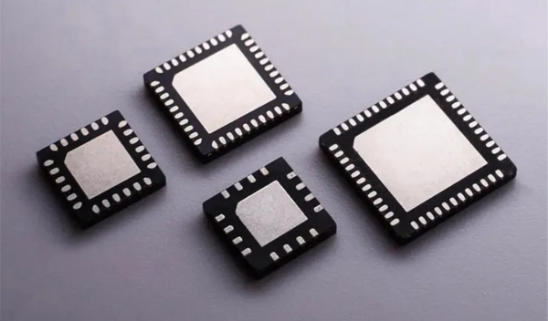
What Size are QFN Packages?
QFN package sizes span a wide range to accommodate various IC complexities and application requirements. Standard dimensions start as small as 1mm × 1mm for ultra-compact low-pin-count devices up to 20mm × 20mm for high-pin-count integrated circuits.
Common mainstream sizes include 3mm × 3mm, 4mm × 4mm, 5mm × 5mm, and 7mm × 7mm, with corresponding pin counts from 8 to 64 pins. Package heights typically range from 0.4mm to 1.8mm, with low-profile variants (LQFN) measuring 0.75mm to 1.0mm thick. Pin pitch (distance between adjacent pads) commonly measures 0.4mm, 0.5mm, or 0.65mm, with fine-pitch versions at 0.3mm for high-density I/O requirements.
What are the Different Types of QFN Packages?
The QFN package family includes several variants optimized for specific performance, manufacturing, and application needs.
- Standard QFN: Basic quad flat no-leads package with perimeter signal pads and central thermal pad.
- LQFN (Low-Profile QFN): Thinner profile (typically <1mm) for height-constrained designs.
- UQFN (Ultra-thin QFN): Extremely low profile (~0.4mm) for ultra-compact portable devices.
- WQFN (Wafer-level QFN): Package size nearly identical to die size for minimal footprint.
- SQFN (Saw-cut QFN): High-precision package with tight dimensional tolerance using saw singulation process.
- PQFN (Punched QFN): Cost-effective package using punch singulation for high-volume production.
- Ceramic QFN: High-temperature performance package using ceramic material for aerospace/automotive.
- Wettable Flank QFN: Side-plated pads enabling visual solder joint inspection for high-reliability applications.
- Dual-row QFN: Double row of perimeter pads for increased I/O density in same package size.
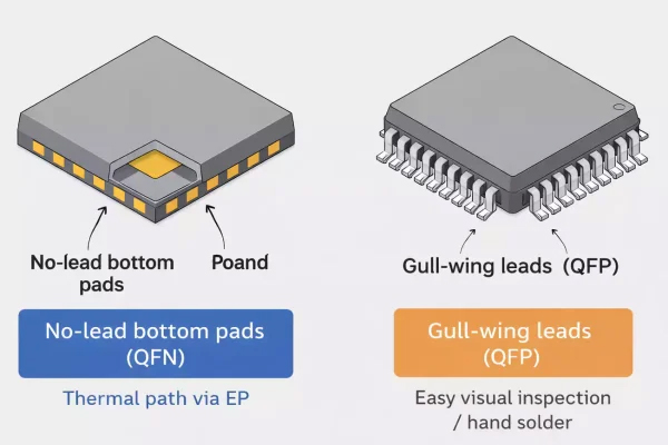
What is the Difference between QFN and QFP Packages?
Here are difference between QFN and QFP packages:
| Characteristic | QFN Package | QFP Package |
|---|---|---|
| Lead Structure | No external leads; bottom pads | Gull-wing leads extending outward |
| Package Size | 40% smaller than equivalent QFP | Larger footprint due to protruding leads |
| Profile Height | 0.4mm – 1.0mm (Low-profile) | 1.0mm – 3.8mm (Thicker) |
| Thermal Performance | Excellent (central thermal pad) | Poor (no dedicated thermal path) |
| Electrical Performance | Superior (low parasitic inductance) | Good (higher parasitic inductance) |
| Inspection | Requires X-ray (joints hidden) | Visual inspection (leads visible) |
| Rework | Difficult (specialized hot air equipment) | Easy (conventional soldering tools) |
| PCB Density | High (small footprint) | Medium (larger footprint) |
| Cost | Lower (material efficient) | Higher (more complex lead forming) |
What is the Difference between DFN and QFN Packages?
Here are difference between DFN and QFN packages:
| Characteristic | DFN Package | QFN Package |
|---|---|---|
| Pad Configuration | Pads on two opposite sides | Pads on all four sides |
| Form Factor | Rectangular (dual-in-line style) | Square or rectangular (quad style) |
| Pin Count | Lower (2 – 24 pins) | Higher (8 – 100 pins) |
| Application | Simple ICs (regulators, MOSFETs) | Complex ICs (microcontrollers, SoCs) |
| Footprint | Compact dual-in-line | Compact quad format |
| Thermal Pad | Available (central) | Standard (central large pad) |
| PCB Space | Minimal for low I/O | Efficient for high I/O |
What is the Difference between LGA Package and QFN Package?
Here are difference between LGA package and QFN package:
| Characteristic | LGA Package | QFN Package |
|---|---|---|
| Contact Type | Bare metal pads (no solder pre-coat) | Solderable pre-coated pads |
| Assembly | Requires solder paste on PCB | Compatible with standard reflow |
| Coplanarity | Critical tolerance demands | More forgiving coplanarity |
| Socket Compatibility | Supports socket mounting | Generally not socket compatible |
| Electrical Contact | Direct metal-to-metal pressure contact | Solder joint connection |
| Thermal Interface | Similar thermal pad performance | Similar thermal pad performance |
| Common Applications | High-performance processors | General-purpose ICs |
What is the Difference between Wlcsp and QFN Packages?
Here are difference between WIcsp and QFN packages:
| Characteristic | WLCSP Package | QFN Package |
|---|---|---|
| Packaging Scale | Wafer-level (no conventional package) | Component-level (molded package) |
| Size | Die-sized (smallest possible) | Slightly larger than die |
| Interconnect | Solder bumps on die surface | Lead frame with bond wires |
| Thickness | Ultra-thin (~0.3mm) | Thin (0.4mm – 1.0mm) |
| Thermal Performance | Good (direct die to PCB) | Excellent (thermal pad) |
| Rework | Extremely difficult | Difficult but feasible |
| Cost | High (wafer-level processing) | Lower (mass production efficient) |
| Production Volume | Medium to high | High volume optimized |
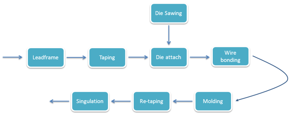
How are QFN Packages Made?
The QFN package process flow involves precise semiconductor packaging techniques.
- Leadframe Preparation: The QFN package uses a C194 or C7025 copper alloy leadframe. Large copper sheets are stamped or etched into a matrix of units (each with perimeter pads and a central thermal pad); etching is preferred for fine-pitch (≤0.4 mm) packages for precision. The leadframe is chemically cleaned to remove oxide and debris for strong adhesion.
- Die Attach: The silicon die is mounted to the leadframe’s thermal pad via conductive epoxy (low-power) or solder paste (high-power). Epoxy is dispensed uniformly (0.05–0.1 mm) and cured (150–180°C, 30–60 minutes); solder paste is reflowed (240–250°C). Poor die attach causes overheating or failure.
- Wire Bonding: 18–25 μm gold, copper, or aluminum wires connect the die’s pads to the leadframe. Gold is for high-reliability uses (automotive/aerospace), copper for cost-sensitive electronics. Ultrasonic bonding forms secure connections; copper clips replace wires for high-pin-count packages. AOI checks for broken wires or poor bonds.
- Mold Encapsulation: The die, wires, and inner leadframe are sealed with epoxy mold compound (EMC, Tg ≥150°C) via transfer molding (10–20 MPa, 170–180°C). The mold leaves perimeter and thermal pads exposed for soldering and heat dissipation; multi-stage injection avoids air bubbles and wire sweep.
- Post-Mold Cure: The assembly is cured at 175–185°C for 2–4 hours to enhance EMC strength and stability, reducing residual stress and delamination risk.
- Singulation: The leadframe matrix is split into individual packages via sawing (precise, for fine-pitch) or punching (faster, for large/low-pin-count). Sawing uses a diamond tip and deionized water coolant; post-singulation inspection checks for cracks or damage.
- Plating: Exposed pads are plated with tin (5–10 μm), NiPdAu (2–5 μm Ni, 0.1–0.3 μm Au), or RoHS-phased tin-lead. NiPdAu is preferred for high reliability due to better corrosion resistance and solderability.
- Testing and Quality Control: QFN packages undergo electrical (continuity, insulation, functional), mechanical (warpage, bond strength), and visual inspections. Qualified packages are sorted and packaged in tape-and-reel for shipment.
How to Solder QFN Package?
Successful QFN package soldering requires precise process control and specialized techniques.
Preparation
- Design PCB with appropriate QFN package footprints, including thermal pad with thermal vias.
- Use laser-cut stencil (0.1mm – 0.12mm thickness) with optimized apertures for signal and thermal pads.
- Apply low-voiding solder paste (SAC305 alloy preferred) with consistent printing pressure.
- Place QFN package with high-accuracy pick-and-place equipment (±0.02mm precision).
Reflow soldering process
- Preheat: 150°C – 180°C for 60 – 90 seconds, ramp rate ≤3°C/s.
- Soak: 180°C – 200°C for 45 – 60 seconds to activate flux.
- Reflow: Peak temperature 235°C – 245°C, time above liquidus 40 – 60 seconds.
- Cool: Controlled cooling (≤4°C/s) to minimize thermal stress.
Inspection
- Use X-ray inspection to verify solder joint quality and void percentage.
- Ensure <15% void area on thermal pad and <5% voids on signal joints for reliability.
What Are Common Issues of QFN Packaging Soldering?
The QFN package presents unique soldering challenges:
Solder Bridging: Adjacent pads shorted by excess solder
- Cause: Excessive paste, poor stencil design
- Fix: Reduce paste volume, optimize stencil openings
Void Formation: Air bubbles in thermal pad solder
- Cause: Trapped flux, insufficient peak temperature
- Fix: Optimize reflow profile, use window-pane stencil design
Poor Wetting: Incomplete solder adhesion
- Cause: Oxidation, insufficient heat
- Fix: Use high-activity paste, ensure proper thermal profiling
Tombstoning: Component lifting on one side
- Cause: Uneven heating, unbalanced paste
- Fix: Optimize reflow uniformity, balance paste distribution
Insufficient Thermal Pad Solder: Poor heat dissipation
- Cause: Inadequate paste deposition
- Fix: Proper stencil design for thermal pad
How Much Does QFN Package Cost?
QFN package pricing varies based on size, pin count, technology, and volume. Standard QFN package costs range from $0.15 to $1.50 per unit in high-volume production (100k+ units). Small 8 – 16 pin QFNs cost $0.15 – $0.30, mid-range 24 – 48 pin versions $0.25 – $0.60, and high-pin-count 64 – 100 pin devices $0.50 – $1.50. Specialized variants (wettable flank, ceramic, ultra-thin) add 20% – 50% premium. Compared to alternatives, QFN package costs 15% – 30% lower than equivalent QFP packages and 30% – 60% lower than WLCSP packages, offering excellent cost-performance value.
FAQs About QFN Packages
Q1: Should You Avoid QFN Packages for Custom PCB?
A1: No, you should not avoid QFN package use for custom PCBs. The QFN package offers significant advantages in size, thermal performance, and electrical efficiency that outweigh assembly challenges for most applications. Avoid QFN package only for low-volume prototypes with limited rework equipment or extremely simple circuits where larger packages suffice. For most modern designs, the QFN package provides optimal benefits with proper PCB design and assembly processes.
Q2: How to Remove QFN Package with Soldering Iron?
A2: Removing a QFN package with a soldering iron is challenging but possible with specialized techniques.
- Preheat entire PCB to 100°C – 120°C to prevent thermal shock.
- Apply generous high-activity flux to all package edges and thermal pad area.
- Use a wide chisel tip (3mm – 5mm) set to 320°C – 350°C.
- Heat alternating package sides continuously while applying gentle upward pressure.
- For thermal pad, use solder wick to remove solder once package is removed.
- Clean pads with flux remover and prepare for reattachment.Note: Hot air rework stations provide superior results for QFN package removal.
Q3: What is the Minimum Pitch for QFN Package?
A3: The minimum standard pitch for QFN package components is 0.3mm, with 0.4mm and 0.5mm being most common. Fine-pitch QFN package variants at 0.3mm demand advanced PCB manufacturing and assembly processes, including precise stencil design, accurate placement, and X-ray inspection.
Q4: Are QFN Packages Suitable for High-Frequency Applications?
A4: Yes, QFN package technology excels in high-frequency applications. The short electrical paths minimize parasitic inductance and capacitance, enabling excellent signal integrity at GHz frequencies. This makes the QFN package ideal for RF transceivers, microwave circuits, and high-speed digital interfaces.
Q5: How Many Thermal Vias Are Needed for QFN Package?
A5: Recommended thermal via count for QFN package ranges from 4 to 16 vias depending on thermal pad size. A 5mm × 5mm QFN package typically uses 9 – 16 vias (0.3mm – 0.4mm diameter) arranged in a grid pattern within the thermal pad to maximize heat transfer to internal PCB planes.
Q6: Can QFN Packages Be Hand Soldered?
A6: Hand soldering QFN package is possible for larger pitch (≥0.5mm) versions but difficult for fine-pitch devices. Success requires fine-tip soldering iron, high-quality flux, magnification, and steady hands. The process involves pre-tinning pads, applying flux, aligning component, and heating all sides simultaneously.
Q7: What is the Shelf Life of QFN Packages?
A7: Standard QFN package components have a 12 – 24 month shelf life when stored in dry conditions (≤5% RH) at 15°C – 25°C. Moisture-sensitive devices require dry storage and baking before assembly if exposed to ambient conditions beyond their floor life.
Q8: Are QFN Packages Reliable for Automotive Applications?
A8: Yes, QFN package variants meet automotive AEC-Q100 standards when properly specified. Wettable flank QFNs enable visual inspection for automotive quality control, while enhanced molding compounds withstand temperature cycling and harsh environments.
Q9: What is the Difference Between MLF and QFN Package?
A9: MLF (Micro Lead Frame) is simply an alternative industry name for QFN package technology. Both terms describe identical quad flat no-leads packaging with bottom pads and central thermal pad, with no functional difference between them.
Q10: Does QFN Package Require Underfill for Reliability?
A10: Underfill is recommended for QFN package in high-reliability applications (automotive, industrial) to enhance thermal cycle performance and mechanical shock resistance. It is optional for consumer electronics but significantly improves long-term durability under stress conditions.