 language
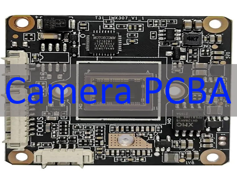
High-Quality Camera PCBA: Comprehensive Solutions for All Camera Types
Camera PCBA serves as the core circuit assembly that powers imaging, signal processing, and stable operation in all camera devices. This article covers definitions, types, high-end standards, fabrication, assembly, supplier selection, thermal and inspection camera applications, and why Best Technology is your trusted manufacturing partner.
Many projects face repeated frustrations with camera circuit board PCBA performance and delivery. What are the most common pain points when developing and sourcing camera module PCBA?
- Unstable imaging caused by poor signal integrity
- Long lead times delaying prototype and mass production
- Inconsistent quality with high defect and rework rates
- Limited miniaturization for micro camera designs
- Unreliable suppliers lacking high-end expertise
We provide targeted, factory-backed solutions to resolve these issues efficiently.
- High-precision impedance control for clean high-speed signals
- Fast PCB assembly and micro camera PCBA prototyping in 1–5 days
- IPC-A-610 Class 2/3 inspection with AOI/X-Ray for consistent quality
- Support for 01005 components and 0.25mm BGA pitch for miniaturization
- 18-year expertise in high-end PCBA camera fabrication and assembly
Best Technology is a professional camera PCBA manufacturer with 20 years of experience in PCB manufacturing and full-turnkey PCBA assembly. We specialize in digital camera PCBA, PCBA thermal camera, PCBA inspection camera, and high-end camera PCBA solutions, holding ISO 9001, ISO 13485, IATF 16949, RoHS, and REACH certifications. Our capabilities include precise PCB fabrication down to 3/3mil line width/spacing, SMT placement for 01005 components, and full in-line quality control. We offer one-stop service from PCB design, manufacturing, component sourcing, PCBA camera assembly to final testing. Pls feel free to contact us at sales@vn.danyupcbs.com for reliable, high-quality camera PCBA solutions.
An Overview of Camera PCBA: Definition and Core Functions
Camera PCBA (Printed Circuit Board Assembly) integrates imaging sensors, processors, power management, and interface circuits onto a camera circuit board PCBA to enable image capture, processing, and transmission.
Core functions:
- Power regulation and noise filtering for stable sensor operation
- High-speed signal transmission for MIPI/LVDS imaging interfaces
- Precise component coordination for real-time image processing
- Mechanical support and thermal management for reliability
- Compatibility with digital, thermal, inspection, and micro camera modules
In short, camera PCBA is the foundational platform that determines imaging quality, stability, and durability across consumer, industrial, and professional applications.
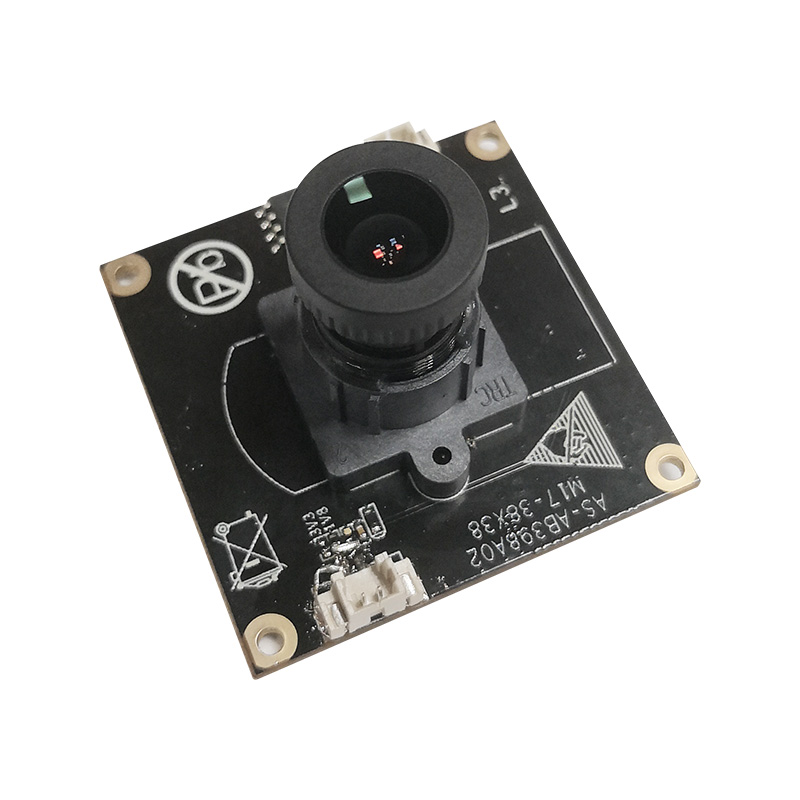
Common Camera PCBA Types: From Digital to Thermal Camera Applications
Camera PCBA covers a wide range of applications, each with distinct design and manufacturing requirements.
Main types:
- Common camera PCBA: Basic consumer cameras, webcams, entry-level devices
- Digital camera PCBA: Compact digital cameras, DSLR/mirrorless supporting boards
- Action camera PCBA: High‑shock, waterproof, portable action cameras for sports and outdoor use
- Dash camera PCBA: In‑car driving recorders with stability, vibration resistance, and low‑light performance
- PCBA thermal camera: Thermal imaging for industry, security, firefighting
- PCBA inspection camera: Endoscopes, machine vision, AOI systems
- Micro camera PCBA: Wearables, drones, medical devices with miniaturized modules
- High-end PCBA camera: Professional broadcast, cinema, industrial precision systems
These types share core assembly processes but differ in materials, layer count, precision, and thermal design.
High-End Camera PCBA: Key Standards and Quality Control Measures
High-end PCBA camera demands strict standards to ensure superior imaging, stability, and longevity.
Key standards and controls:
- Material: High-Tg FR4, Rogers, Isola for thermal stability and signal integrity
- Line width/space: Inner/outer layer down to 3/3mil for high-density routing
- Surface finish: ENIG (Ni 3–8μm, Au 0.025–0.125μm) for corrosion resistance
- Assembly: IPC-A-610 Class 2/3, 01005 placement, 0.25mm BGA pitch
- Inspection: 3D SPI, 3D AOI, X-Ray for BGA void control and defect prevention
- Testing: Functional test, thermal cycling, vibration for reliability
Quality control runs from incoming materials to final shipment, ensuring PCBA for camera high-end performance.
Camera Module PCBA Supplier: How to Choose a Reliable Partner
Selecting the right camera module PCBA supplier directly impacts project success.
Key evaluation points:
- Technical capability: Support for micro, high-end, thermal, and inspection camera PCBA
- Quality system: Certifications (ISO 9001, IATF 16949) and IPC standards
- Supply chain: Authorized component channels (Digi‑Key, Mouser, Avnet)
- Service model: Full turnkey, fast prototyping, flexible volume support
- Experience: Track record in digital camera PCBA and PCBA thermal camera projects
- Communication: Responsive engineering and project management
Prioritize suppliers with end-to-end control and proven camera PCBA expertise.
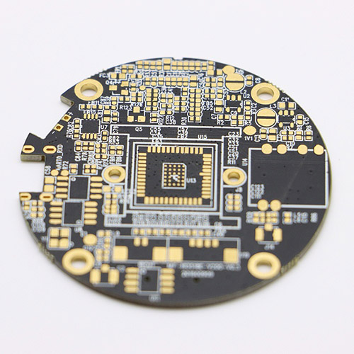
PCBA Camera Fabrication & Assembly: Process and Technical Points
PCBA camera fabrication and assembly require precision engineering to meet imaging and reliability demands.
PCB Fabrication
- Materials: FR4 Standard/Medium/High-Tg, high-frequency laminates
- Layers: 1–32 layers; 8+ layers use High-Tg
- Line width/space: Conventional 4/4mil; special 3/3mil
- Board thickness: 0.2–3.5mm; ultra-thin down to 0.15mm
- Surface finish: OSP, ENIG, immersion silver/tin, NiPdAu, gold fingers
PCBA Assembly Process
- DFA and incoming material inspection
- SMT stencil manufacturing and solder paste printing
- 3D SPI inspection
- SMD placement (01005, BGA 0.25mm pitch)
- Reflow soldering
- 3D AOI and X-Ray inspection
- THT insertion and wave soldering
- Functional test, cleaning, final inspection
Our fast PCB assembly micro camera PCBA prototyping service supports rapid validation in 1–5 days.
PCBA Thermal Camera: Market Demand
PCBA thermal camera is growing rapidly in industrial monitoring, safety, medical, and automotive sectors.
Market demand drivers:
- Infrared temperature measurement for equipment predictive maintenance
- Night vision and perimeter security
- Building diagnostics and electrical fault detection
- Medical thermal screening
- Automotive driver assistance
As a professional PCBA thermal camera factory and supplier, we support:
- High-performance thermal sensor integration
- Low-noise power design
- Enhanced thermal management
- Compliance with industrial and medical standards
PCBA Inspection Camera: Application Scenarios and Technical Advantages
PCBA inspection camera supports visual inspection across electronics manufacturing, medical, and industrial automation.
Key applications:
- PCB/PCBA production AOI and solder joint inspection
- Medical endoscopy and minimally invasive surgery
- Industrial robotic vision and quality control
- Narrow-space equipment maintenance
- Security and surveillance detail capture
Technical advantages:
- Miniaturized design for tight spaces
- High-resolution, low-distortion imaging
- Stable high-speed data transmission
- Anti-interference and long-term reliability
- Customizable for fixed or mobile inspection
What Makes Best Technology the Ideal Partner for Camera PCBA Manufacturing?
We stand out as a trusted camera PCBA manufacturer with comprehensive advantages.
- 20 years of expertise in digital camera PCBA, PCBA thermal camera, PCBA inspection camera
- Full turnkey service from design to shipment
- Advanced equipment: 3D SPI, 3D AOI, X-Ray, high-speed placement
- Stringent quality: IPC standards, ISO/IATF certifications, RoHS/REACH
- Fast delivery: Prototyping 1–5 days, mass production on time
- Competitive pricing via efficient process and cost control
- Professional support for micro, high-end, and custom camera PCBA
To sum up, camera PCBA is the critical circuit assembly that ensures imaging performance, stability, and reliability across all camera devices. This article has explained definitions, types, high-end standards, fabrication, assembly, supplier selection, thermal and inspection camera applications, and the strengths of Best Technology. With 20 years of experience, advanced equipment, strict quality control, and full-turnkey service, we deliver high-quality, reliable camera PCBA solutions for digital, thermal, inspection, micro, and high-end applications. For inquiries about camera circuit board PCBA, camera module PCBA, PCBA camera fabrication, or fast prototyping, pls feel free to contact us at sales@vn.danyupcbs.com.
FAQs About Camera PCBA
Q: What is the difference between common camera PCBA and high-end PCBA camera?
A: High-end versions use better materials, finer line width, stricter assembly, and higher testing standards for superior image quality and reliability.
Q: How fast can you provide micro camera PCBA prototyping?
A: Our fast PCB assembly micro camera PCBA prototyping service takes 1–5 days.
Q: Do you support PCBA thermal camera and PCBA inspection camera orders?
A: Yes, we are a professional thermal camera PCBA supplier and inspection camera PCBA manufacturer.
Q: What quality standards do you follow?
A: IPC-A-610, AS9100D, ISO 9001, ISO 13485, IATF 16949, RoHS, REACH.
Q: Can you handle both small prototypes and mass production?
A: Yes, we support flexible volumes from prototypes to large batches.