 language
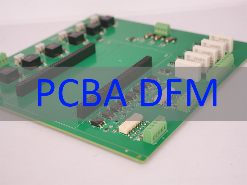
Mastering PCBA DFM: Essential Guidelines for Optimal Manufacturing
PCBA DFM (Design for Manufacturing) is a critical engineering practice that aligns PCB design with real‑world assembly capabilities to boost yield, cut costs, and speed up production. This blog breaks down core definitions, principles, actionable PCBA DFM guidelines, common pitfalls, engineer roles, workflow integration, benefits, tools, and FAQs to help you build fully manufacturable PCBAs.
Many design teams face avoidable headaches during PCB assembly. Are you struggling with these common challenges?
- Designs fail SMT assembly due to incompatible footprints or spacing
- BGA, 01005, and fine‑pitch components cause high rework and low yield
- Long lead times and repeated prototype revisions delay product launches
- Unclear PCB fabrication and assembly rules lead to miscommunication and errors
- High costs from rework, scrap, and last‑minute design changes
At Best Technology, we solve these pain points with structured, factory‑proven DFM support.
- Free professional PCBA DFM review before production
- Strict adherence to IPC standards and our in‑house PCB & PCBA capabilities
- Dedicated DFM PCBA engineer for personalized design optimization
- Clear, actionable PCBA DFM guidelines tailored to SMT/THT/mixed assembly
- One‑stop turnkey service with 1–5 day lead time and 97% on‑time delivery
Best Technology is a trusted PCB and PCBA manufacturer with 20+ years of expertise, serving 1,700+ clients across 40 countries. We provide full turnkey solutions including PCB design, fabrication, component sourcing, SMT/THT assembly, and testing. Our ISO 9001, ISO 13485, IATF 16949, RoHS, and REACH certifications ensure consistent quality. We support FR‑4, metal‑based, flexible, rigid‑flex, high‑frequency, and ceramic PCBs, with advanced lines handling 01005 components, 0.25 mm BGA pitch, and high‑precision assembly. Professional PCBA DFM review is available upon contact at sales@vn.danyupcbs.com.
What Is PCBA DFM and Why It Matters?
PCBA DFM refers to design rules and checks that optimize printed circuit board assemblies for reliable, cost‑effective, and efficient manufacturing. It bridges design intent and factory reality by accounting for equipment limits, material constraints, and assembly processes.
Key reasons PCBA DFM is non‑negotiable:
- Reduces assembly defects, rework, and scrap
- Lowers total production cost and shortens lead times
- Improves yield, especially for fine‑pitch, BGA, and miniaturized designs
- Ensures compatibility with SMT, THT, and mixed assembly lines
- Supports consistent quality aligned with IPC standards
In short, PCBA DFM turns theoretical designs into producible, reliable products.
Core Principles of DFM for PCBA
Effective DFM for PCBA follows stable, repeatable principles that match our factory capabilities.
- Align with real manufacturing limits: Match trace/space, hole sizes, BGA pitch, and component clearances to our PCB and PCBA process specs.
- Simplify for automation: Optimize for pick‑and‑place, solder paste printing, reflow, and AOI/X‑ray inspection.
- Prioritize yield and reliability: Avoid tombstoning, solder bridging, cold joints, and insufficient clearance.
- Standardize components and footprints: Use IPC‑7351 land patterns and readily available parts to reduce shortages.
- Design for inspection and test: Enable AOI, X‑ray, and functional testing early in layout.
- Maintain thermal balance: Use thermal reliefs and proper via design to avoid soldering defects.
These principles form the foundation of our internal PCBA DFM guidelines.
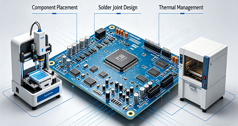
Key PCBA DFM Guidelines for Design Success
Follow these factory‑validated rules to achieve stable, high‑yield PCBA production.
Component & Placement Rules
- Support 01005 minimum SMD and 0.25 mm minimum BGA pitch
- Maintain minimum clearance per package type
- Keep polarized components consistently oriented
- Avoid components too close to board edges (risk of depaneling damage)
- Follow IPC‑7351 for all land pattern design
PCB Layout & Tolerance Rules
- Trace/space matches our copper weight capabilities (1–20 oz)
- Hole size and aspect ratio comply with drilling capabilities
- Minimum annular ring and drill‑to‑copper spacing observed
- Solder mask clearance and bridge width follow assembly standards
- Silkscreen kept 0.15 mm+ from pads; no overlapping pads
Stencil, Solder & Thermal Rules
- Stencil thickness and aperture optimized for component pitch
- Thermal relief pads for large copper planes
- Vias not placed in BGA thermal pads to prevent solder voids
- Reflow profile designed for board complexity and layer count
Material & Finish Rules
- Use FR‑4, high‑TG, high‑frequency, ceramic, or metal‑core materials matched to performance needs
- Surface finish: ENIG, immersion tin/silver, OSP, HASL, etc., suitable for assembly
- Compliance with RoHS and REACH requirements
Following these PCBA DFM guidelines drastically reduces assembly issues.
Common DFM Issues in PCBA and How to Avoid
Most assembly failures stem from avoidable design errors. Below are the top problems and fixes.
| DFM Issue | Root Cause | Prevention |
|---|---|---|
| Solder bridging | Insufficient mask clearance, tight pad pitch, poor stencil design | Follow mask rules; use correct stencil apertures |
| Tombstoning | Unequal pad size, unbalanced thermal relief, poor reflow | Symmetric pads; thermal relief optimization |
| BGA voids & opens | Vias in thermal pad, uneven paste, poor stencil | No vias in pad; optimized paste printing |
| Component misalignment | Bad fiducials, tight spacing, panel distortion | Clear fiducials; follow placement clearance |
| Silkscreen errors | Overlapping pads, tiny text, low contrast | Keep 0.15 mm clearance; min height 0.7 mm |
| Drill violations | Small holes with thick boards, tight hole‑to‑copper | Follow aspect ratio and clearance rules |
Our DFM PCBA engineer catches these issues during pre‑production review.
Role of a DFM PCBA Engineer in Production
A dedicated DFM PCBA engineer is critical to bridging design and manufacturing.
Key responsibilities:
- Conduct full PCBA DFM review against IPC and factory standards
- Optimize footprints, clearances, stencil design, and thermal layout
- Collaborate with designers to resolve layout conflicts
- Create and update PCBA DFM guidelines and checklists
- Support NPI, prototype, and mass production ramp
- Troubleshoot assembly defects and implement corrective actions
- Train teams on DFM for PCBA best practices
At Best Technology, every project gets expert DFM support to ensure success.
DFM Check Process in PCB Assembly Workflow
Our structured DFM workflow ensures zero avoidable errors.
- Design Submission: Receive Gerber, BOM, centroid, and drill files.
- Preliminary DFM Scan: Automated check for clearances, trace/space, hole sizes, and silkscreen issues.
- DFA & Component Check: Verify parts availability, packaging, and assembly compatibility.
- Detailed Engineering Review: DFM PCBA engineer checks BGA, fine‑pitch, thermal, and stencil design.
- Report & Revision Support: Share clear PCBA DFM report with actionable fixes.
- Final Approval: Design frozen after confirmation; released to production.
This process ensures your board runs smoothly on our SMT/THT lines.
Benefits of Implementing PCBA DFM Standards
Strong PCBA DFM delivers measurable business improvements.
- Lower cost: Reduce scrap, rework, and prototype iterations
- Faster launch: Shorten lead times to 1–5 days; 97% on‑time delivery
- Higher yield: Improve first‑pass yield for fine‑pitch and complex boards
- Better quality: Stable, reliable assemblies per IPC and customer specs
- Simplified supply chain: One‑stop turnkey service with transparent WIP updates
- Scalability: Designs ready for prototype to mass production
DFM for PCBA is not extra cost—it is high‑impact investment.
Tools & Best Practices for PCBA DFM Optimization
Use these tools and habits to strengthen your DFM process.
DFM Software Tools
- Valor NPI, CAM350, and CAD DRC modules
- 3D SPI/AOI/X‑ray visualization
- IPC‑7351 footprint libraries
Best Practices
- Run DFM early and often in design cycle
- Use manufacturer’s PCBA DFM guidelines before finalizing layout
- Standardize footprints and approved components
- Simulate reflow and thermal performance
- Review panelization, fiducials, and test points
- Partner with an experienced EMS with in‑house DFM support
These steps ensure your design is truly assembly‑ready.
In summary, PCBA DFM is the foundation of high‑yield, low‑cost, reliable PCB assembly, aligning design with real manufacturing capabilities. This blog has covered definitions, core principles, key PCBA DFM guidelines, common issues, DFM PCBA engineer roles, workflow integration, benefits, tools, and FAQs to support your design success.
Best Technology combines 20+ years of expertise, advanced SMT lines, strict quality certifications, and dedicated DFM support to deliver turnkey PCB and PCBA solutions. We ensure your designs are optimized for performance, cost, and speed. For a free PCBA DFM review or project quote, pls feel free to contact us at sales@vn.danyupcbs.com.
FAQs About PCBA DFM
Q: What is the difference between DFM and DFA for PCBA?
A: DFM (Design for Manufacturing) covers PCB fabrication; DFA (Design for Assembly) focuses on component mounting. PCBA DFM combines both.
Q: When should I perform a PCBA DFM check?
A: Before releasing Gerber/BOM files; before prototype and mass production.
Q: What is the most critical DFM rule for SMT?
A: Correct IPC‑7351 footprints and sufficient clearance for 01005/BGA.
Q: Does Best Technology provide free PCBA DFM reviews?
A: Yes—we offer free consultation and full DFM analysis for all customers.
Q: How long does a PCBA DFM check take?
A: Typically 1–2 business days for standard designs.