 language
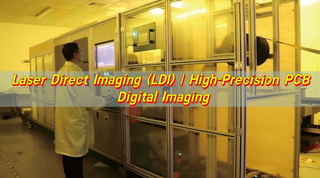
Laser Direct Imaging (LDI) | High-Precision PCB Digital Imaging
Advanced laser direct imaging (LDI) technology for PCB manufacturing, delivering ultra-fine line resolution, maskless exposure, high alignment accuracy and fast production cycles.
What is laser direct imaging?
Laser direct imaging, often abbreviated as LDI, is a modern digital imaging technology used to transfer circuit patterns onto printed circuit boards (PCBs) without the need for traditional phototools or film masks. Instead of relying on physical artwork, LDI uses a focused laser beam controlled by digital data to expose photoresist directly on the PCB surface.
This shift from analog to digital imaging has transformed how circuit patterns are created. In traditional processes, any design change required a new photomask, which increased both cost and lead time. With laser direct imaging, design files can be updated instantly, allowing manufacturers to respond faster to engineering changes.
At its core, LDI improves alignment accuracy, reduces defects, and supports finer line widths. These advantages make it especially valuable for high-density interconnect (HDI) boards and advanced multilayer designs. As electronic devices become smaller and more complex, the demand for precise imaging continues to grow, and LDI meets this demand effectively.
Another key aspect of LDI is its ability to compensate for material distortion. PCB materials can expand or shrink slightly during processing. LDI systems can adjust the imaging data in real time, ensuring that the final pattern remains accurate even under variable conditions. This capability is difficult to achieve with traditional exposure methods.
In simple terms, laser direct imaging replaces film with data and replaces light exposure with laser precision. This change may sound small, but its impact on quality, efficiency, and flexibility is significant.
What is LDI in PCB manufacturing?
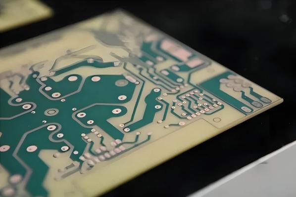
In PCB manufacturing, LDI refers to the specific stage where circuit patterns are transferred onto a photoresist-coated board using laser technology. This step is critical because it defines the electrical pathways that will later be etched into copper layers.
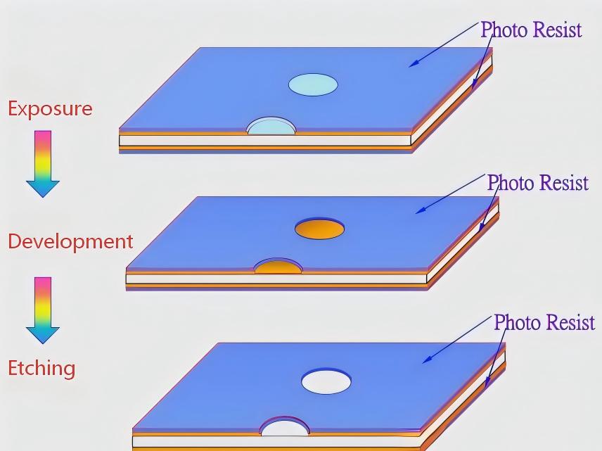
The LDI process typically takes place after the board has been cleaned and coated with photoresist. The machine reads digital design files, often in Gerber format, and uses a laser to expose the pattern directly onto the board. After exposure, the board goes through a development process where the unexposed or exposed areas are removed, depending on the type of resist used.
LDI is used in several stages of PCB production, including:
- Inner layer imaging for multilayer boards
- Outer layer imaging for final circuit definition
- Solder mask imaging for precise mask openings
Compared to conventional exposure systems, LDI offers better control over critical dimensions. This is especially important for fine-pitch components and high-speed circuits, where even small deviations can affect performance.
For manufacturers like Best Technology, integrating LDI into PCB production lines allows for tighter tolerances and improved consistency across batches. It also supports quick-turn prototyping, which is essential for customers developing new products under tight deadlines.
What is the wavelength of laser direct imaging?
The wavelength used in laser direct imaging typically falls within the ultraviolet (UV) range. Most LDI systems operate using lasers with wavelengths around 355 nm or 405 nm, depending on the machine design and photoresist compatibility.
These wavelengths are chosen because they provide high energy and fine resolution. Shorter wavelengths allow the laser to create smaller features with sharper edges, which is essential for modern PCB designs.
Here are some common wavelength ranges used in LDI systems:
- 355 nm (UV laser): widely used for high-resolution applications
- 375–405 nm (near-UV): used in systems that balance cost and performance
- Advanced systems may use multiple wavelengths for different layers
The choice of wavelength affects several factors:
- Resolution capability
- Exposure speed
- Compatibility with different photoresists
- Equipment cost
UV lasers are particularly effective because they interact well with photoresist materials. This ensures clean exposure and reduces the risk of undercutting or incomplete development. In practical terms, the wavelength determines how fine the circuit lines can be. As PCB designs move toward smaller geometries, the importance of shorter wavelengths becomes more evident.
How does an LDI work?
Understanding how LDI works helps explain why it delivers such precise results. The process combines digital data processing, optical systems, and motion control to create accurate circuit patterns.
The workflow of an LDI system can be described in several key steps:
- Data preparation: The PCB design file is loaded into the LDI system and processed for imaging
- Alignment: The board is positioned using reference points to ensure accurate placement
- Laser exposure: A focused laser beam scans across the surface, exposing the photoresist according to the design
- Dynamic scaling: The system adjusts for material distortion in real time
- Development: The board is developed to reveal the pattern
Unlike traditional exposure systems that use a single flash of light through a mask, LDI uses a scanning approach. The laser moves across the board in a controlled pattern, ensuring that each feature is precisely defined.
One of the most valuable features of LDI is its ability to perform automatic optical alignment. The system detects fiducial marks on the board and adjusts the imaging position accordingly. This reduces misalignment issues, especially in multilayer boards.
Additionally, LDI systems often include advanced software that can modify exposure parameters on the fly. This allows for consistent results even when working with different materials or environmental conditions. For manufacturers aiming to deliver high-reliability PCBs, this level of control is essential. It ensures that each board meets strict quality standards without excessive rework.
What is the difference between VDI and LDI?
VDI, or vector direct imaging, and LDI are both digital imaging technologies used in PCB manufacturing. While they share some similarities, their approaches and applications differ in important ways.
VDI uses vector-based data to control the imaging process, often focusing on drawing lines and shapes directly. LDI, on the other hand, uses raster-based imaging, where the laser scans the surface line by line.
Here is a clear comparison:
| Aspect | VDI (Vector Direct Imaging) | LDI (Laser Direct Imaging) |
|---|---|---|
| Imaging method | Vector drawing | Raster scanning |
| Data format | Vector data | Rasterized image data |
| Speed | Faster for simple designs | Consistent for complex designs |
| Resolution | Good for standard patterns | Excellent for fine features |
| Flexibility | Limited for dense layouts | Highly flexible |
| Application | Simpler PCBs | HDI and multilayer PCBs |
VDI can be efficient for straightforward designs, but it may struggle with very dense or complex patterns. LDI provides more consistent results across different design types, making it the preferred choice for advanced applications. In modern PCB manufacturing, LDI has largely become the standard due to its versatility and precision.
What is the difference between LDA and LDI?
LDA, or laser direct ablation, is another laser-based process used in PCB manufacturing. While it may sound similar to LDI, the two technologies serve different purposes.
LDI is used for imaging, meaning it exposes photoresist to define patterns. LDA, in contrast, removes material directly using a laser, without the need for photoresist or chemical development.
Here is a detailed comparison:
| Aspect | LDA (Laser Direct Ablation) | LDI (Laser Direct Imaging) |
|---|---|---|
| Process type | Material removal | Photoresist exposure |
| Use of chemicals | Not required | Required (development stage) |
| Application | Drilling, structuring | Circuit imaging |
| Precision | High, but limited by material | Very high for fine lines |
| Cost | Higher equipment cost | Balanced cost and performance |
| Typical use | Flexible circuits, special layers | Standard PCB imaging |
LDA is often used in specialized applications, such as creating microvias or removing dielectric layers. LDI, however, remains the primary method for defining circuit patterns. Both technologies can coexist in advanced manufacturing environments, each serving its own role.
Can LDI improve PCB production quality?
LDI has a direct and measurable impact on PCB production quality. Its precision and consistency help reduce defects and improve overall yield. One of the main quality improvements comes from better alignment. Misalignment between layers can cause electrical failures. LDI minimizes this risk through accurate positioning and real-time adjustments.
Another benefit is improved line definition. Fine خطوط and spaces are more consistent, which is essential for high-speed and high-frequency circuits. This leads to better signal integrity and reduced interference.
LDI also reduces common defects such as:
- Open circuits caused by incomplete exposure
- Short circuits due to pattern distortion
- Registration errors in multilayer boards
For companies like Best Technology, adopting LDI means delivering products that meet strict international standards. It also reduces the need for rework, which saves time and lowers production costs.
In addition, LDI supports better repeatability. Each board is produced using the same digital data, ensuring uniform quality across large production runs. Overall, LDI enhances both reliability and performance, making it a key technology in modern PCB fabrication.
What are the main benefits of using LDI for PCBs?
The benefits of LDI go beyond basic imaging. It offers a combination of precision, efficiency, and flexibility that is difficult to achieve with traditional methods.
Some of the most important advantages include:
- High precision: Supports fine and tight spacing
- No photomasks: Eliminates the need for film, reducing cost and lead time
- Fast design changes: Digital files can be updated instantly
- Better alignment: Reduces layer misregistration
- Improved yield: Fewer defects and less rework
In addition to these technical benefits, LDI also supports modern manufacturing trends. For example, it enables rapid prototyping, which is critical for product development cycles.
Another advantage is scalability. Whether producing a small batch or a large volume, LDI maintains consistent quality. This makes it suitable for both prototype and mass production environments.
From a business perspective, LDI helps manufacturers stay competitive. It reduces operational costs while improving product performance, which is a strong combination in the electronics industry. At Best Technology, integrating LDI into PCB production lines allows for faster delivery, higher accuracy, and better customer satisfaction. This aligns with the growing demand for reliable and high-performance electronic products.
Summary:
Laser direct imaging is a powerful technology that has reshaped PCB manufacturing by replacing traditional film-based processes with precise digital exposure. It improves accuracy, supports complex designs, and reduces production time.
From understanding its working principles to comparing it with VDI and LDA, it is clear that LDI offers significant advantages in both quality and efficiency. Its ability to handle fine features and adapt to material variations makes it essential for modern electronics.
For manufacturers and engineers, adopting LDI is not just an upgrade but a strategic step toward better performance and reliability.
If you are looking for high-quality PCB solutions with advanced imaging technology, feel free to reach out to Best Technology at sales@bestpcb.vn.