 language
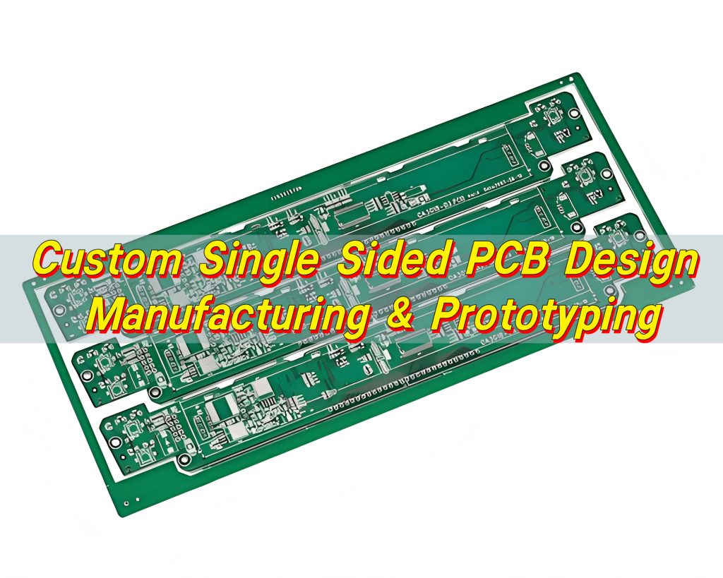
Custom Single Sided PCB Design | Manufacturing & Prototyping
Single sided PCB design refers to the process of designing printed circuit boards with conductive traces on only one side of the substrate, typically used for simple, cost-sensitive electronic applications.
In many real projects, engineers still rely on single-sided boards for cost control, fast prototyping, and stable mass production. However, challenges such as routing limitations, trace congestion, and manufacturability constraints often slow down development.
Are you facing these common challenges in single sided PCB design?
- Difficulty routing signals without crossing traces
- Limited space for component placement
- Uncertainty in trace width and current capacity
- Confusion between single layer and multi-layer trade-offs
- Concerns about reliability and scalability
The good news is that with proper design rules and manufacturing support, these challenges can be effectively managed. A well-optimized single layer PCB can still deliver excellent performance, especially when supported by an experienced manufacturing partner like Best Technology.
What is a single-sided PCB?
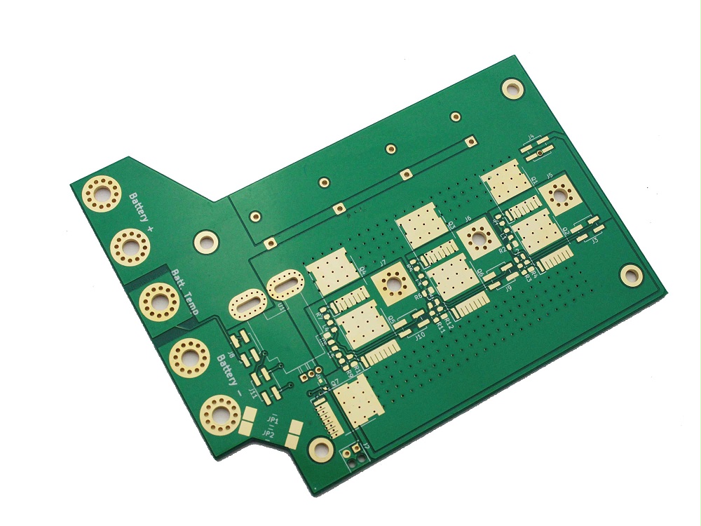
A single-sided PCB, also known as a single layer PCB, consists of a base substrate (usually FR4 or phenolic material) with a conductive copper layer on only one side. All components and routing are implemented on this single conductive surface.
Unlike double sided or multi layer PCB structures, there are no plated through holes for signal routing between layers. This makes the structure simple, but also places higher demands on layout planning.
A typical single sided PCB structure includes:
- Substrate layer (FR4, CEM-1, or aluminum for thermal designs)
- Copper layer (usually 1 oz, sometimes 2 oz for power applications)
- Solder mask layer
- Silkscreen for component identification
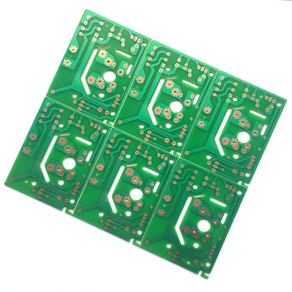
Because of its simplicity, this type of PCB is widely used in high-volume, low-cost electronics where circuit complexity is limited.
At Best Technology, we frequently support customers who require fast prototyping and low-cost single layer PCB fabrication, especially for consumer electronics and industrial control modules.
Basic rules for single sided PCB layout design
Designing a single sided PCB requires more discipline than multi-layer designs, because routing options are limited. Every decision must consider manufacturability and electrical performance.
Here are several core layout rules that engineers should follow:
- Keep signal paths short and direct to reduce resistance and noise
- Place components logically to minimize routing complexity
- Group related components together to simplify connections
- Avoid unnecessary vias, since they increase cost in single layer boards
- Maintain consistent trace widths for predictable current flow
In addition, designers often use jumpers or zero-ohm resistors to bridge unavoidable crossovers. While this adds slight assembly complexity, it allows routing flexibility without moving to a double layer PCB.
What is a single-sided PCB used for?
Single sided PCBs remain highly relevant in many industries due to their simplicity and cost efficiency. They are especially suitable for applications where circuit density is low and reliability is critical.
Common applications include:
- Consumer electronics (remote controls, toys, simple chargers)
- LED lighting modules and power drivers
- Household appliances such as washing machines and fans
- Industrial control panels with basic logic circuits
- Power supply units with straightforward topology
In these applications, using a multi layer PCB would unnecessarily increase cost without delivering meaningful benefits. For example, LED driver boards often use single sided PCB design combined with aluminum substrate to improve thermal dissipation while maintaining low production cost.
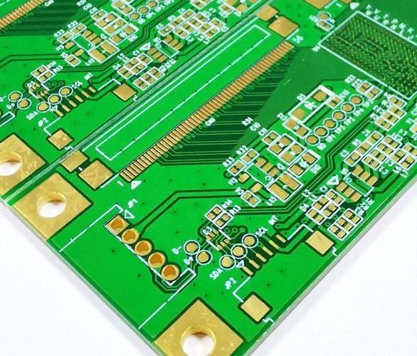
Trace width and spacing in single sided PCB design
Trace width and spacing are critical parameters that directly affect electrical performance, thermal behavior, and manufacturability.
In single sided PCB design, proper trace sizing becomes even more important because all current flows through one layer.
Typical guidelines include:
- Standard signal traces: 6–10 mil width
- Power traces: 20–100 mil depending on current
- Minimum spacing: 6–8 mil for standard fabrication
- High voltage spacing: increased according to safety standards
When designing for higher current, engineers must calculate trace width carefully to prevent overheating. Increasing copper thickness (e.g., 2 oz instead of 1 oz) is another effective solution.
A practical approach is to combine wider traces with short routing paths, which improves both electrical efficiency and thermal stability.
How to avoid cross traces in single sided PCB design?
One of the biggest challenges in single sided PCB design is avoiding trace intersections, since there is only one conductive layer.
Engineers typically use several techniques to solve this problem:
- Optimize component placement early in the design phase
- Rotate components to align pins for easier routing
- Use jumper wires or zero-ohm resistors when necessary
- Route critical signals first before less important ones
For more complex circuits, designers may consider slight redesign of the schematic to reduce routing conflicts. While avoiding cross traces entirely is ideal, controlled use of jumpers is widely accepted in production, especially for cost-sensitive projects.
How thick is a single sided PCB?
The thickness of a single sided PCB depends on both mechanical and electrical requirements. Standard thickness values are widely used in the industry for compatibility and cost control.
Common thickness ranges include:
- 0.8 mm (thin designs for compact devices)
- 1.0 mm to 1.6 mm (most common standard)
- 2.0 mm and above (for mechanical strength or power applications)
Copper thickness also plays an important role:
- 1 oz (35 µm): standard applications
- 2 oz (70 µm): higher current handling
- 3 oz and above: heavy copper designs
Thicker boards provide better mechanical rigidity, while thinner boards reduce weight and material cost. The optimal choice depends on the specific application.
What is the difference between single-sided PCB and double-sided PCB?
Single sided and double sided PCBs differ mainly in structure, routing capability, and application scope. A single sided PCB has only one copper layer, while a double sided PCB includes conductive layers on both sides, connected through plated vias.
Below is a clear comparison:
| Feature | Single Sided PCB | Double Sided PCB |
|---|---|---|
| Copper Layers | 1 layer | 2 layers |
| Routing Complexity | Limited | Moderate |
| Manufacturing Cost | Lower | Higher |
| Design Flexibility | Low | Higher |
| Use Cases | Simple circuits | More complex systems |
| Assembly | Easier | Slightly more complex |
In practice, engineers often start with a single layer PCB and upgrade to double layer PCB design only when routing becomes too complex.
What are the disadvantages of single layer PCB?
While single sided PCBs offer many advantages, they also have limitations that must be considered during design.
Key constraints include:
- Limited routing space, which restricts circuit complexity
- Difficulty handling high-density components
- Reduced flexibility for future upgrades
- Potential need for jumpers in complex layouts
Despite these limitations, careful design can still achieve excellent performance for suitable applications. In fact, many engineers prefer single layer PCB solutions for stable, high-volume products where simplicity reduces failure rates.
Common mistakes in single sided PCB design and how to avoid them
Even experienced designers can encounter issues when working with single sided PCB layouts. Understanding common mistakes helps avoid costly redesigns.
Here are several typical errors and solutions:
- Poor component placement leading to routing congestion
- Using trace widths that are too narrow for current requirements
- Ignoring thermal effects in power circuits
- Overusing jumpers instead of optimizing layout
- Not considering manufacturing tolerances
To avoid these problems:
- Start with a clear layout strategy before routing
- Validate current paths and thermal load early
- Follow standard design rules and spacing guidelines
- Collaborate with your PCB manufacturer for DFM review
At Best Technology, we provide free DFM feedback to help customers identify and resolve these issues before production.
Conclusion:
Single sided PCB design remains a practical and efficient solution for many electronic applications. When designed carefully, it offers a strong balance between cost, reliability, and manufacturability.
If you are planning a project and want to ensure fast turnaround, stable quality, and cost-effective production, working with an experienced manufacturer is essential. Best Technology has over 19 years of experience in PCB fabrication and assembly, offering one-stop services from design support to full turnkey production. We support prototypes, small batches, and mass production with consistent quality and fast delivery.
For professional support or a quick quote, feel free to contact: sales@bestpcb.vn