 language
How to Choose Printed Circuit Board Thickness | Custom PCB Sizes
What is the thickness of a printed circuit board?
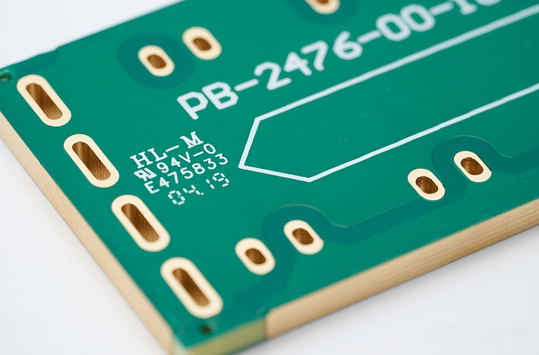
Printed circuit board thickness refers to the total vertical dimension of a PCB, including substrate material, copper layers, prepreg, and surface finishes. It is one of the most fundamental parameters in PCB design because it directly affects mechanical strength, electrical performance, and manufacturability.
In most standard applications, the standard printed circuit board thickness is 1.6 mm (approximately 0.063 inches). This value is widely accepted across industries because it balances rigidity, cost efficiency, and compatibility with connectors and enclosures. However, this is only a reference point rather than a strict limitation.

A typical standard PCB thickness chart looks like this:
| PCB Type | Common Thickness | Typical Use |
|---|---|---|
| 2 Layer PCB | 0.8 mm / 1.0 mm / 1.2 mm / 1.6 mm | Consumer electronics, IoT |
| 4 Layer PCB | 1.2 mm / 1.6 mm / 2.0 mm | Industrial control, telecom |
| 6+ Layer PCB | 1.6 mm – 3.2 mm | High-speed, complex systems |
| Ultra-thin PCB | 0.2 mm – 0.6 mm | Wearables, compact devices |
| Thick PCB | 2.4 mm – 6.0 mm+ | Power electronics |
The printed circuit board thickness standards are not universal rules but industry practices based on fabrication capabilities and application needs. Designers often choose thickness based on mechanical requirements, impedance control, and thermal considerations.
At Best Technology, engineers frequently assist customers in selecting thickness based on real-world usage rather than theoretical values. This approach reduces redesign cycles and improves product reliability from the first build.
How thick can you make a PCB?
PCB thickness can go far beyond standard values when required by specific applications. In practice, thick PCBs can reach 3.2 mm, 4.0 mm, or even over 6.0 mm depending on structural and electrical demands.
These thicker boards are often used in:
- Power electronics systems
- Automotive control units
- High-current applications
- Industrial machinery
A thicker PCB typically includes:
- More dielectric layers
- Increased copper thickness
- Reinforced core materials
However, increasing thickness is not simply stacking materials together. It requires careful control of lamination pressure, resin flow, and layer alignment. Otherwise, internal stress may affect long-term reliability.
Here is a quick comparison:
| Thickness Range | Advantages | Trade-offs |
|---|---|---|
| 1.6 mm | Balanced performance | Limited mechanical strength |
| 2.4–3.2 mm | Stronger structure | Higher cost |
| 4.0 mm+ | High rigidity, high power | Complex manufacturing |
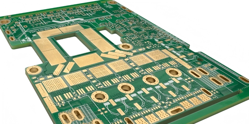
Best Technology has experience producing heavy copper and thick boards up to high ounce copper structures, ensuring stable performance in demanding environments.
How thin can a PCB be?
On the opposite end, ultra-thin PCBs are becoming increasingly popular in compact electronics. These boards can be as thin as 0.2 mm or even thinner in specialized designs.
Thin PCBs are commonly used in:
- Wearable devices
- Medical electronics
- Flexible and rigid-flex products
- Consumer gadgets
Their benefits include:
- Reduced weight
- Compact size
- Improved flexibility
However, thin boards require strict process control. Warpage, handling damage, and assembly challenges are more common compared to standard boards.
Typical thin PCB thickness ranges:
| Category | Thickness |
|---|---|
| Ultra-thin rigid PCB | 0.2 – 0.4 mm |
| Standard thin PCB | 0.6 – 1.0 mm |
| Flexible PCB | <0.2 mm |
In practical engineering scenarios, selecting a thinner board must be balanced with mechanical durability and assembly requirements such as SMT processes.
How to measure printed circuit board thickness accurately?
Accurate measurement of printed circuit board thickness is essential for quality control and compliance with design specifications.
The most commonly used methods include:
- Digital micrometer: High precision, suitable for finished boards
- Caliper measurement: Quick inspection for general tolerance checks
- Cross-section analysis: Used in labs for detailed layer measurement
- Thickness gauge systems: Used in production lines for batch verification
When measuring PCB thickness, it is important to consider:
- Solder mask contribution
- Surface finish thickness (ENIG, HASL, etc.)
- Copper plating variation
Typical printed circuit board thickness tolerance is:
- ±10% for standard boards
- ±0.1 mm for precision designs
For high-reliability industries such as medical or aerospace, tighter tolerances are required, often validated through controlled inspection processes and traceability systems.
Why are some printed circuit board traces thicker than others?
Trace thickness is different from board thickness, but both are closely related in PCB design.
The printed circuit board copper thickness determines how much current a trace can carry. Thicker copper allows higher current flow and better heat dissipation.
Common copper thickness values:
| Copper Weight | Thickness |
|---|---|
| 1 oz | 35 µm |
| 2 oz | 70 µm |
| 3 oz | 105 µm |
| 4 oz+ | 140 µm+ |
Reasons for varying trace thickness:
- High current requirements
- Thermal management needs
- Voltage drop reduction
- Reliability improvements
For example, power supply circuits often use thicker traces, while signal lines remain thinner for precision.
At Best Technology, heavy copper PCBs can reach up to high ounce levels, supporting demanding applications such as power modules and industrial control systems.
What is the 3W rule in PCB?
The 3W rule is a guideline used in PCB layout to reduce signal interference. It states that the spacing between two parallel traces should be at least three times the width of the trace.
This rule helps minimize:
- Crosstalk
- Electromagnetic interference
- Signal integrity issues
For example:
- If trace width = 0.2 mm
- Minimum spacing = 0.6 mm
Although modern high-density designs may not always follow this rule strictly, it remains a useful reference for improving signal quality.
How to choose PCB thickness?
Choosing the right printed circuit board thickness is not about following a standard value. It is about matching the board structure with the application requirements.
A practical approach includes:
- Define mechanical strength requirements
- Consider connector compatibility
- Evaluate electrical performance
- Analyze thermal behavior
- Review manufacturing constraints
For most applications:
- 1.6 mm works well for general electronics
- 1.2 mm is suitable for compact designs
- 2.0 mm+ is preferred for high-power systems
A structured decision process reduces risk and ensures consistent product performance.
Factors that affect printed circuit board thickness selection
Several factors influence thickness selection, and they often interact with each other.
Key factors include:
- Layer count: More layers typically increase thickness
- Material type: FR4, Rogers, ceramic, or metal core
- Copper thickness: Heavier copper adds to total thickness
- Application environment: Temperature, vibration, and stress
- Assembly method: SMT, through-hole, or mixed
For example, high-frequency PCBs may require specific thickness to maintain controlled impedance, while power boards prioritize thermal dissipation.
Best Technology supports a wide range of materials including FR4, metal core, ceramic, and high-frequency substrates, allowing flexible thickness customization for different industries.
PCB thickness vs mechanical strength and stability
PCB thickness plays a direct role in mechanical performance. Thicker boards generally offer better rigidity and resistance to bending.
Here is a clear comparison:
| Thickness | Mechanical Strength | Flexibility |
|---|---|---|
| Thin (≤1.0 mm) | Low | High |
| Standard (1.6 mm) | Balanced | Moderate |
| Thick (≥2.4 mm) | High | Low |
Thicker boards are ideal for:
- Large PCBs
- Heavy components
- Harsh environments
Thin boards are preferred for:
- Compact devices
- Lightweight applications
- Flexible designs
Selecting the right balance ensures durability without unnecessary cost.
How does thickness affect thermal performance of PCBs?
Thermal performance is closely related to both PCB thickness and copper structure.
Thicker PCBs can:
- Improve heat spreading
- Support higher power loads
- Reduce thermal hotspots
However, thermal efficiency also depends on:
- Material thermal conductivity
- Copper weight
- Design layout
For example:
- Metal core PCBs provide superior heat dissipation
- Ceramic PCBs offer excellent thermal conductivity
- Thick copper layers enhance heat transfer
In high-power designs, thickness alone is not enough. A well-optimized structure combining material selection and copper distribution delivers the best results.
Summary:
Printed circuit board thickness is a critical parameter that influences mechanical strength, electrical behavior, and thermal performance. While 1.6 mm remains the most common standard, real-world applications often require customized thickness to meet specific design goals.
Choosing the right thickness involves understanding multiple factors, including layer count, copper weight, material type, and operating environment. Both thin and thick PCBs have their advantages, and the best choice depends on the application rather than a fixed standard.
At Best Technology, with over 19 years of experience in PCB fabrication and assembly, engineers provide tailored recommendations to help customers achieve optimal performance and reliability. If you are unsure about the right PCB thickness for your project, feel free to reach out for expert support:
sales@vn.danyupcbs.com