 language
What is Ceramic Package?
A ceramic package —sometimes called a ceramic housing or ceramic enclosure—is a protective shell made from advanced ceramic materials. It safeguards delicate semiconductors and microelectronic components from heat, moisture, and physical damage. Inside this enclosure, the chip is securely held and electrically connected to external circuits, maintaining stability even under severe environmental conditions.
Compared with plastic or epoxy-based housings, ceramic packaging stands out for its exceptional durability and heat resistance. That’s why it’s the go-to choice for high-end industries such as aerospace, defense, medical, automotive, and telecommunication sectors. As devices continue to shrink in size yet expand in performance, the need for packaging that can survive high temperature and pressure becomes more essential than ever—and ceramic materials meet that challenge perfectly.
Raw Materials Used in Ceramic Packaging
The reliability of a ceramic package starts from its foundation—the raw materials. Each material contributes unique mechanical, electrical, and thermal properties that determine how well the final package performs.
Alumina (Al₂O₃) is the most widely used base ceramic. It offers excellent electrical insulation, mechanical strength, and moderate thermal conductivity, making it the preferred material for most standard ceramic housings. Its balance between performance and cost efficiency makes it a universal choice across industries.
For more advanced applications requiring superior heat transfer, beryllium oxide (BeO) and aluminum nitride (AlN) are adopted. BeO provides outstanding thermal control but must be handled carefully due to its toxic nature in powdered form. Meanwhile, AlN delivers high thermal conductivity with complete electrical insulation, ideal for high-frequency or power semiconductor packages.
To complete the structure, glass frits are introduced to create air-tight seals during firing. These prevent moisture penetration and mechanical failure. For electrical connections, metallization materials such as tungsten (W), molybdenum (Mo), or platinum (Pt) are printed on ceramic surfaces. Their thermal expansion closely matches the ceramic body, minimizing stress and preventing cracks during thermal cycling.
Key Features of Ceramic Packages
- High Airtightness: Hermetic sealing keeps moisture, dust, and gases away from sensitive chips.
- Excellent Thermal Conductivity: Rapid heat dissipation keeps devices operating safely at high temperatures.
- Outstanding Mechanical Strength: Resistant to micro-cracking, vibration, and mechanical shock.
- Superior Electrical Insulation: Prevents signal interference and leakage even in dense circuit designs.
- Thermal Expansion Compatibility: Ceramic’s expansion rate closely matches silicon, minimizing stress between chip and package.
- Low Moisture Permeability: Essential for long-term reliability, especially in space or medical applications.
- Flexible Structural Design: Capable of complex, multi-dimensional wiring structures that support advanced circuit integration.
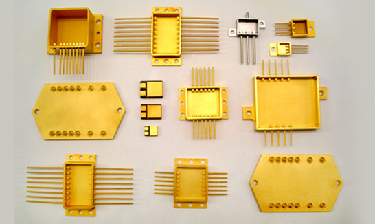
Types of Ceramic Packages
Ceramic packaging covers a wide range of configurations designed for different circuit requirements and performance levels. The most common types include:
1. Ceramic Dual Inline Package (CERDIP)
One of the earliest ceramic designs, the CERDIP features two rows of metal pins extending from a rectangular ceramic body. Inside, the chip is sealed with glass or metal lids for protection. While less common today, CERDIPs remain popular in aerospace and defense applications where failure is not an option.
2. Ceramic IC Package
This broad category covers any ceramic-based housing for integrated circuits. Ceramic IC packages come in multiple shapes and interfaces, including flatpacks, pin grid arrays (PGA), and ball grid arrays (BGA). They are highly valued in high-speed and high-frequency electronics due to minimal signal loss and low dielectric constant.
3. LTCC Package (Low Temperature Co-Fired Ceramic)
LTCC technology builds multi-layer circuits by stacking and co-firing ceramic tapes at about 850°C. Conductive patterns are printed between layers, and passive components such as resistors or capacitors can be embedded directly inside. LTCC packages are compact, lightweight, and ideal for RF modules, wireless systems, and satellite communications.
4. HTCC Package (High Temperature Co-Fired Ceramic)
The HTCC process involves firing at higher temperatures—around 1600°C—using materials like tungsten or molybdenum. These packages are extremely robust and suited for power modules, EV control systems, and military electronics where both mechanical and thermal endurance are critical.
Other common shapes and structures include:
- Ceramic Pin Grid Array (CPGA)
- Ceramic Quad Flat Package (CQFP)
- Ceramic Land Grid Array (CLGA)
- Ceramic Flat Package (CFP)
- Dual In-line Ceramic Package (CDIP)
- Multi-Chip Module (MCM / MMIC)
- Ceramic Quad Flat No-Lead Package (CQFN)
- Butterfly Shell for optical applications
Each of these structures offers specific advantages depending on the design complexity, power requirements, and intended operating environment.
LTCC vs. HTCC Ceramic Packages
While both LTCC and HTCC involve co-firing ceramic layers, their differences determine their ideal applications:
| Feature | LTCC | HTCC |
| Firing Temperature | <1000°C | >1600°C |
| Metals Used | Gold, silver | Tungsten, molybdenum |
| Circuit Density | High; supports embedded passive components | Simpler; designed for rugged, large modules |
| Applications | Telecom, sensors, RF modules | Power electronics, aerospace, defense |
| Cost | Slightly higher due to gold and embedded parts | Lower for simpler designs, but higher for large rugged modules |
LTCC excels in compact, high-frequency designs. HTCC is better for mechanically tough and high-power applications.
Ceramic Packaging Manufacturing Process
The manufacturing of a ceramic package is a highly precise and multi-step process. Each stage contributes to the package’s reliability, thermal performance, and mechanical strength. Modern production relies on strict control over materials, temperature, and alignment to produce high-quality LTCC and HTCC packages. Here’s a detailed look at the process:
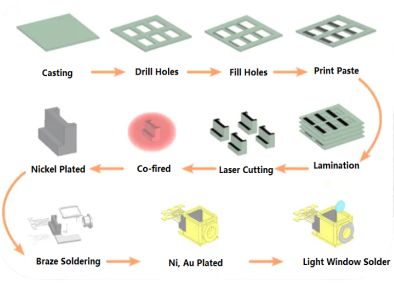
1. Tape Casting
The process begins with ceramic tape casting, which forms the foundation of the package. Fine ceramic powders such as alumina (Al₂O₃), aluminum nitride (AlN), or beryllium oxide (BeO) are mixed with binders and solvents to form a slurry.
- The slurry is spread into thin, uniform sheets on a flat surface using a casting blade or automated tape casting machine.
- After drying, these sheets are flexible enough for handling yet retain enough strength to support later processing steps.
- The thickness of the tape is carefully controlled, as it determines the final package height and layer precision.
These sheets, often called green tapes, will later form the multilayer structure of the ceramic package.
2. Hole Drilling (Vias Formation)
Once the green tapes are ready, tiny holes known as vias are created to enable vertical electrical connections between the layers:
- Drilling is done using either mechanical drills for larger vias or laser drilling for microvias.
- The diameter, placement, and alignment of the vias are critical because they directly affect electrical performance and reliability.
- After drilling, the vias are cleaned to remove debris and ensure proper filling in the next step.
3. Filling the Vias
Drilled vias are filled with a conductive paste, typically made from tungsten, molybdenum, or gold-based materials depending on the firing temperature and application requirements.
- This paste will form the internal electrical pathways during co-firing.
- Proper filling ensures consistent conductivity and prevents voids, which could compromise the package’s performance.
- In LTCC, silver or gold paste is often used; in HTCC, tungsten or molybdenum is preferred due to higher firing temperatures.
4. Printing Circuit Patterns
Next, the surface of each ceramic layer is printed with circuit patterns using screen printing or other precision deposition techniques:
- Conductive traces, pads, and ground planes are applied at this stage.
- This step also allows integration of passive components in LTCC packages, such as capacitors or resistors.
- Proper alignment is critical to avoid misconnection when layers are stacked.
5. Lamination
The prepared ceramic layers are stacked in the correct sequence to form a multilayer block and then laminated under heat and pressure:
- Lamination ensures that all layers bond tightly and maintain precise alignment.
- Temperature and pressure settings are optimized based on the type of ceramic material.
- This step forms a rigid, unified structure ready for firing.
6. Laser Cutting / Pre-Firing Shaping
Before firing, the laminated block is often cut using a laser to define the package outline and any alignment notches or openings:
- Laser cutting provides precise, clean edges and shapes.
- In packages with optical or sensor functions, windows or apertures are also created at this stage.
7. Co-Firing
The stacked and laminated block undergoes co-firing in a high-temperature furnace to sinter the ceramic layers and solidify the conductive pathways:
- HTCC firing: Around 1600°C using coarse ceramic powders and refractory metals (tungsten/molybdenum).
- LTCC firing: Around 850°C using fine ceramic tapes and low-resistance metals (silver/gold).
- Co-firing transforms the green tape into a dense, hard ceramic body while integrating the conductive traces into a single, reliable structure.
8. Surface Plating (Nickel Plating)
After firing, exposed metal pads and vias are nickel-plated. Nickel serves as a barrier layer to prevent oxidation and improve solderability. This step is critical for the long-term reliability of electrical connections, especially in harsh environments.
9. Braze Soldering
Any metal parts, such as lids, lead frames, or support structures, are attached using brazing. High-temperature alloys create a strong, hermetic seal between metal and ceramic.
10. Ni/Au Plating
To further improve solderability and corrosion resistance, the connection areas are plated with a thin layer of gold over nickel:
- Ni/Au plating is ideal for wire bonding or flip-chip mounting.
- Gold ensures long-term electrical stability and prevents oxidation during use.
11. Light Window Solder (Optional)
For packages that require optical access, such as sensors or LEDs, a transparent window is added. The window is soldered or bonded precisely to ensure optical clarity and hermetic sealing. Common in LTCC packages for RF, optical, or sensor applications.
12. Final Inspection and Testing
Every ceramic package undergoes rigorous quality control:
- Dimensional inspection ensures precise alignment and size.
- Electrical tests verify continuity, insulation, and signal integrity.
- Thermal and mechanical stress tests simulate real-world conditions.
The ceramic packaging manufacturing process is highly detailed and requires precision at every stage—from raw material selection to final testing. Each step contributes to the package’s reliability, thermal performance, and mechanical strength, which is why ceramic packages are preferred in aerospace, defense, medical, automotive, and high-performance electronics.
At Best Technology, we combine advanced LTCC and HTCC processes with strict quality control and customization capabilities to deliver ceramic packages that meet even the most demanding requirements.
Applications of Ceramic Packages
Ceramic packages are used in areas where failure is not an option:
- Aerospace & Satellites: Power modules, guidance systems, radar electronics
- Military Equipment: Secure communications, radar, missile guidance
- Medical Devices: Pacemakers, sensors, diagnostic equipment
- Telecommunications: LTCC modules for 5G, antennas, amplifiers
- Automotive Electronics: HTCC packages in EVs, hybrid systems, and battery monitoring
- Industrial Automation: Sensors, actuators, motor controllers
Ceramic Package vs. Ceramic PCB
Because both use ceramic materials, ceramic packages are often confused with ceramic PCBs, but they serve entirely different roles in an electronic system.
| Aspect | Ceramic Package | Ceramic PCB |
| Definition | A sealed enclosure that houses and protects a semiconductor chip. | A ceramic-based printed circuit board that supports and connects multiple components. |
| Primary Function | Protects the chip and provides external electrical connection. | Provides electrical pathways between multiple devices. |
| Structure | Fully enclosed and hermetically sealed. | Open surface board with printed or buried circuits. |
| Thermal Performance | High heat resistance and moderate dissipation. | Very high thermal conductivity (especially AlN). |
| Moisture Protection | Completely sealed against moisture and gases. | Not hermetic; surface coating may offer partial protection. |
| Size and Design | Compact, chip-level housing. | Larger board accommodating several active and passive parts. |
| Assembly Method | Wire bonding, brazing, or flip-chip mounting. | SMT or through-hole soldering. |
| Cost Level | Generally higher due to complexity and precision. | Lower to moderate, depending on layers and material. |
Why Choose Best Technology for Ceramic Package Solutions?
At Best Technology, we specialize in custom ceramic packaging that meets the most demanding technical and environmental requirements. From concept to production, our engineering team provides comprehensive support in material selection, structural design, and prototype development.
We are capable of producing both LTCC and HTCC ceramic packages, along with hybrid solutions tailored to your specific application. Our advanced manufacturing systems and strict quality controls ensure precision and reliability in every product we deliver.
What We Offer:
- Expertise in ceramic IC package design, customization, and assembly.
- Access to premium materials such as Al₂O₃, BeO, and AlN.
- Flexible production volumes—from prototype to mass manufacturing.
- Complete Ni/Au plating, brazing, and hermetic sealing capabilities.
- ISO9001, ISO13485, IATF16949, and AS9100D certified facilities for aerospace, automotive, and medical sectors.
- Full MES traceability and global customer support.
When you need packaging that delivers stability, heat resistance, and electrical excellence, you can rely on Best Technology. We help turn innovative ideas into durable, real-world solutions—built to last in the most demanding environments.