 language
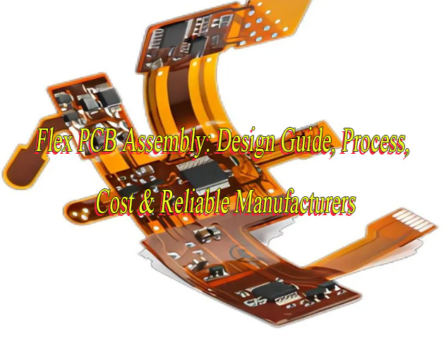
Flex PCB Assembly: Design Guide, Process, Cost & Reliable Manufacturers
Are you having trouble getting consistent quality and efficiency with your flex PCB assembly projects, and trying to avoid expensive mistakes and delays? This guide focuses on practical, actionable tips for flex PCB assembly from how flex PCBs are manufactured and how to optimize their design, to controlling costs and choosing the right manufacturer. It helps you handle flex PCB assembly easily, avoid costly errors, and stay within budget. You’ll find clear guidance to fix common flex PCB assembly issues, improve project efficiency, and ensure reliable results for both small prototype orders and large bulk orders.
What Is Flex PCB Assembly?
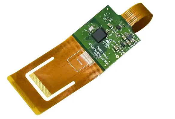
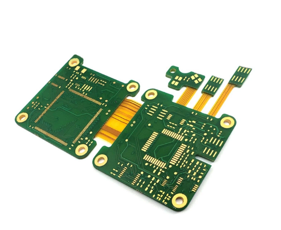
Flex PCB assembly is the process of mounting electronic components onto flexible printed circuit boards, which use bendable substrates like polyimide to fit tight, dynamic spaces. Unlike rigid boards, flex circuits can bend, fold, or twist without damaging connections, making them ideal for wearables, medical devices, automotive systems, and compact electronics.
The process requires specialized handling to ensure component placement and soldering precision. Even well-designed flex circuits can fail without careful assembly, as flexible materials are prone to warping during heat cycles. Successful Flex PCB Assembly combines specialized fixtures, precision equipment, and strict quality checks to deliver reliable performance in high-stress environments.
How Does Flex PCB Assembly Differ From Rigid PCB Assembly?
Below is a comparsion chart between flex PCB assembly and rigid PCB assembly:
| Comparison Dimension | Flex PCB Assembly | Rigid PCB Assembly |
| Substrate Material & Flexibility | Uses bendable substrates like polyimide; can bend, fold, or twist without damage | Uses stiff FR4 material; cannot bend or flex |
| Assembly Handling & Equipment | Requires specialized fixtures to prevent warping; needs precise operation | Follows standard pick-and-place reflow processes; minimal special handling |
| Cost (Material & Total System) | Material costs 4-10× higher than rigid FR4 but reduces total system costs by eliminating connectors/cables | Lower material costs but may increase overall system costs with extra connectors/cables |
| Design Flexibility & Space Saving | Offers 3D design flexibility; saves up to 60% space compared to rigid boards | Limited to flat 2D designs; occupies more space |
| Defect Risk & Precision Requirement | Higher precision required; risk of solder joint failure in bend zones if improperly assembled | Lower precision requirement; fewer defects during assembly |
How Does the Flexible PCB Fabrication Process Work Step by Step?
A complete step by step process of flexible PCB fabrication ensures consistency for both prototype and bulk orders. Each step is critical to avoid defects and ensure the final flex PCB performs reliably in application. Below is the full detailed breakdown of the flexible PCB fabrication process.
- Pre-Production Preparation: Evaluate design manufacturability, prepare polyimide/polyester substrates, copper foil, and adhesive. Process CAD/Gerber files to match equipment specs and create production guidelines.
- Adhesive/Seed Coating: Apply epoxy/acrylic adhesive or sputter copper seed layer to substrate. Ensures strong substrate-copper bonding for flexibility/durability.
- Copper Foil Lamination: Laminate copper foil to adhesive layer or chemically plate copper on seed layer. Adhesiveless lamination of rolled annealed copper enhances flexibility for repeated bending.
- Drilling: Use mechanical drilling for standard holes (multi-layer simultaneous) or laser drilling for ultra-small holes (high precision, single-layer).
- Plating: Clean/activate holes, then copper-plate inner walls for layer-to-layer connectivity. Add nickel/gold/tin to pads for solderability/corrosion resistance.
- Etching: Apply photoresist, expose via photomask, remove unexposed areas, then etch excess copper. Strict time/temperature control prevents circuit weakness or shorts.
- Coverlay Application: Laminate protective polyimide coverlay with precise pad openings. Ensures circuit insulation and environmental protection without copper exposure.
- Surface Treatment: Apply immersion gold, ENIG, or tin plating to pads based on application needs (e.g., corrosion resistance, solder joint reliability).
- Testing: Conduct electrical testing (continuity/shorts), visual/AOI inspection, X-ray (via integrity), and flex-cycle testing for critical applications.
- Singulation: Laser-cut or die-cut individual units from panels. Clean and prepare for assembly—laser for complex shapes, die-cutting for high volume.
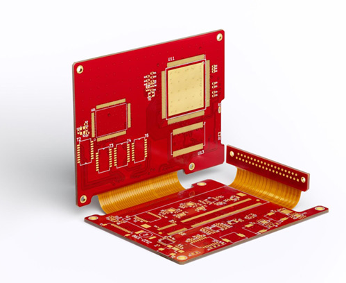
Flex PCB Design Guide: Key Rules for High Yield & Reliability
- Material Selection & Compatibility: Use polyimide (PI) substrates for thermal stability and flexibility. Match copper foil thickness (12-70µm) to bending requirements—thinner for dynamic flexing, thicker for static applications. Ensure adhesive/coverlay materials bond securely without delamination during bending.
- Circuit Design for Flexibility: Design trace widths ≥100µm with spacing ≥100µm to prevent cracking in bend zones. Avoid right-angle turns; use curved routing to distribute stress. Place critical components away from high-flex areas to minimize solder joint fatigue.
- Bend Radius & Mechanical Constraints: Maintain minimum bend radius ≥10x substrate thickness to prevent micro-cracking. Use “teardrop” pads at bend zones to reduce stress concentration. Specify static vs. dynamic flex requirements, dynamic applications require stricter bend radius controls.
- Pad & Via Design for Durability: Size pads ≥200µm diameter for reliable soldering. Use non-penetrating vias (blind/buried) in flex zones to avoid plating cracks. Add solder mask dams between pads to prevent bridging during assembly.
- Coverlay & Stiffener Integration: Apply polyimide coverlay with precise pad openings (±25µm tolerance) to protect circuits without exposing copper. Use FR4 or polyimide stiffeners at connector areas to prevent pad lifting during mating.
- Assembly Process Optimization: Use carrier jigs to stabilize flex boards during SMT. Control reflow temperature ≤260°C to avoid substrate degradation. Apply underfill adhesive at high-stress connectors to enhance mechanical reliability.
- Testing & Validation Protocols: Conduct 100% electrical testing (continuity/shorts) using flying probes. Perform AOI to detect pad misalignment or coverlay defects. Validate bend life with ≥10,000 flex cycles for dynamic applications.
- Design for Manufacturing (DFM) Rules: Include fiducial marks for precise component placement. Use panelization with breakaway tabs to simplify singulation. Provide Gerber files with layer stackup details and assembly drawings for clear communication with manufacturers.
How to Find Reliable Flex PCB Assembly Manufacturers?
Below is a detailed selection guide to flex PCB assembly factory:
- Verify Quality Certifications: Prioritize manufacturers with ISO 9001 ISO 13485 and IATF 16949 certifications. Ensure compliance with IPC-A-610 Class 2 or Class 3 standards as these certifications reduce defect rates by up to 35 percent. Look for additional certifications like UL and ROHS for broader market compliance.
- Check Specialized Equipment and Capabilities: Confirm the manufacturer has dedicated flex PCB assembly equipment including specialized fixtures fine-pitch SMT capabilities down to 0.3mm and flex specific handling tools. Manufacturers with advanced equipment such as laser drilling machines and automated optical inspection systems achieve a 28 percent higher yield rate than those with basic equipment.
- Evaluate Production Capacity and Lead Times: Verify the manufacturer can handle your order size from prototypes to bulk orders. Ideal lead times for prototypes are 2 to 4 days for single or double layer flex PCBs and 5 to 6 days for 4 to 8 layer boards. For bulk orders ensure they can deliver 100000 plus units per month with transparent lead times and backup production lines to avoid delays.
- Assess Quality Control Processes: Reliable manufacturers implement rigorous quality control including AOI X-ray and functional testing. They should have a defect rate below 0.5 percent and provide detailed inspection reports for each production batch. Look for manufacturers that conduct 100 percent electrical testing to ensure continuity and avoid short circuits.
- Confirm Traceability and Documentation: Ensure the manufacturer provides full traceability for all materials and production processes. This includes batch records for raw materials like polyimide substrates and copper foil as well as detailed process logs. Traceability reduces the risk of recall by 40 percent and simplifies troubleshooting if issues arise.
- Check Industry Experience: Prioritize manufacturers with experience in your specific industry such as automotive medical or wearables. Manufacturers with industry specific experience have a 30 percent lower error rate as they understand the unique requirements and standards for each sector.
What Services Do Professional Flex PCB Assembly Factory Provide?
Professional flex PCB assembly factories offer end-to-end services to simplify the process and ensure quality. Below are services that flex PCB assembly factory provide:
- BOM Review and Component Sourcing: BOM review identifies potential issues (e.g., incompatible components) and optimizes part selection. Authorized component sourcing ensures genuine parts, reducing the risk of failures.
- Stencil Design and Fixture Setup: Custom stencils for precise solder paste application and flex-specific fixtures to secure substrates during assembly, preventing warping and misplacement.
- SMT Assembly and Reflow Soldering: High-speed pick-and-place machines for accurate component placement, followed by controlled reflow soldering to ensure strong solder joints without damaging flex substrates.
- Testing and Conformal Coating: Functional testing, ICT, and flying probe testing verify performance. Conformal coating is available to protect assemblies from moisture and environmental damage.
What Factors Influence Flex PCB Assembly Price for Prototype and Bulk Orders?
Understanding the factors that affect flex PCB assembly pricing is essential for budgeting and planning projects effectively. Below are the main elements that impact costs for both prototype and bulk orders, with clear, practical details to help you anticipate expenses.
- Order Volume: Prototype orders (typically 1 to 100 units) have higher per-unit costs because they require setup fees for equipment, stencils, and process preparation. Bulk orders (1000 units or more) benefit from economies of scale, as setup costs are spread across more units, leading to a 30 to 50 percent reduction in per-unit pricing. Small batch orders (101 to 999 units) fall between these two ranges, with moderate per-unit costs.
- Substrate and Material Choices: Polyimide substrates, which offer better flexibility and heat resistance, are more expensive than polyester substrates. Adhesiveless copper foil, often used for high-reliability applications, adds to costs compared to standard adhesive-backed copper. Additionally, specialized coverlays and solder masks designed for dynamic or harsh environments increase material expenses.
- Design Complexity: Fine-pitch components (0.3mm or smaller) require more precise placement equipment and longer assembly time. Multi-layer flex PCBs (more than 4 layers) are more costly to assemble than single or double-layer boards. Laser drilling for microvias, necessary for high-density designs, adds 20 to 30 percent to fabrication and assembly costs compared to mechanical drilling.
- Component Type and Sourcing: High-performance components, rare parts, or components with strict quality standards (such as those for medical or automotive use) are more expensive. Lead-free components, which are required for most modern applications, may also have a slight cost premium over traditional leaded components.
- Testing Requirements: Basic electrical testing (continuity and short-circuit checks) is standard, but advanced testing methods like X-ray inspection, functional testing, or flex cycle testing add to costs. Industry-specific certifications (such as those for medical or aerospace applications) also require additional testing steps, increasing overall expenses.
- Lead Time: Rush orders with shorter lead times (less than 3 days for prototypes or less than 10 days for bulk orders) often include a premium fee. Standard lead times (4 to 7 days for prototypes, 10 to 20 days for bulk) are more cost-effective, as they allow manufacturers to schedule production efficiently without overtime or expedited processes.
- Surface Treatment Options: Immersion gold and electroless nickel immersion gold (ENIG) are more expensive than tin plating but offer better solderability and corrosion resistance. The choice of surface treatment depends on application needs, but each option impacts the total assembly price.
How to Reduce Cost in Flex PCB Assembly Without Losing Quality?
Cost control is achievable in flex PCB assembly without compromising quality. Below are practical, actionable strategies to reduce expenses while maintaining performance and reliability.
- Optimize Material Usage: Utilize intelligent panelization to maximize material utilization, which can increase efficiency by 15%. Intelligent panelization systems automatically generate optimal layouts to minimize waste, supporting two-level panelization and custom parameter settings for better material savings. Choose standard materials where possible, polyester is a cost-effective alternative to polyimide for applications that do not require high-temperature resistance.
- Simplify Design Where Possible: Replace full flex designs with rigid-flex designs in cases where flexibility is only needed in specific areas; this adjustment can reduce material costs by up to 20%. Avoid unnecessary fine-pitch components if standard-sized components meet application requirements, as fine-pitch parts increase assembly time and cost without added value for non-high-density designs.
- Consolidate Orders: Combine prototype and bulk orders with the same manufacturer to eliminate duplicate setup fees, which are a significant cost driver for small orders. Long-term partnerships with manufacturers often lead to volume discounts and more favorable pricing, further reducing overall assembly costs.
- Optimize Testing Processes: For low-volume orders, use automated optical inspection (AOI) combined with flying probe testing instead of more expensive in-circuit testing (ICT). For bulk orders, implement statistical process control to reduce testing time and costs without sacrificing quality, ensuring consistent performance while minimizing redundant checks.
FAQs About Flex Printed Circuit Board Assembly
Q1: What materials are best for flex PCB assembly to ensure durability?
A1: Polyimide (PI) substrates are ideal due to their thermal stability and flexibility. Pair with rolled annealed copper (12-70µm thickness) for dynamic bending applications, thinner copper handles repeated flexing, while thicker copper suits static designs. Adhesiveless lamination reduces delamination risks, enhancing long-term reliability.
Q2: How do I determine the minimum bend radius for my flex circuit?
A2: Maintain a bend radius ≥10x the substrate thickness to prevent micro-cracking. For dynamic applications (e.g., repeated bending), use stricter controls, teardrop-shaped pads at bend zones reduce stress concentration. Static designs can tolerate slightly larger radii but always validate via flex-cycle testing.
Q3: What assembly challenges are unique to flex PCBs versus rigid boards?
A3: Flex circuits require specialized carrier jigs during SMT to prevent warping. Reflow temperatures must stay ≤260°C to avoid degrading polyimide. Solder joint fatigue in bend zones demands precise pad design (≥200µm diameter) and underfill adhesives for high-stress connectors.
Q4: How can I ensure reliable electrical performance in flex zones?
A4: Use curved trace routing (avoid right angles) and ≥100µm trace width/spacing to distribute stress. Non-penetrating vias (blind/buried) in flex zones prevent plating cracks. Solder mask dams between pads prevent bridging during assembly.
Q5: What tests validate flex PCB reliability before deployment?
A5: Essential tests include 100% electrical testing (continuity/shorts via flying probes), AOI for pad/coverlay alignment, and X-ray inspection for via integrity. For dynamic applications, conduct ≥10,000 flex-cycle tests to simulate real-world bending stresses.