 language
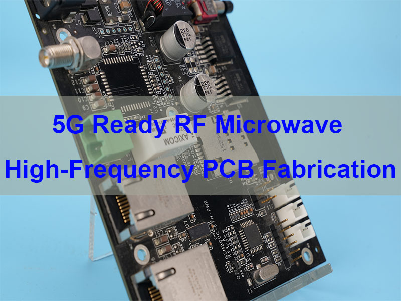
High Frequency RF PCB Fabrication for 5G and Microwave Applications
5G ready RF microwave high-frequency PCB fabrication refers to the manufacturing of printed circuit boards designed to operate reliably at radio frequency and microwave ranges used in modern wireless systems. These PCBs enable stable signal transmission in applications such as 5G base stations, satellite communication equipment, radar modules, and advanced IoT devices.
This article explains the essential principles behind high-frequency PCB fabrication and highlights several engineering calculations that designers and manufacturers use to ensure stable RF performance. If your project involves 5G, RF, or microwave electronics, working with an experienced manufacturing partner can make the development process far more efficient. Best Technology provides 5g ready RF microwave high-frequency PCB fabrication together with complete PCBA assembly support, helping engineers move smoothly from design validation to production. For technical discussion or a quotation, you are welcome to connect with our team at sales@bestpcb.vn or +84-827-237566.
Why 5G Systems Require High-Frequency RF PCB Fabrication?
5G networks operate across multiple frequency bands, including:
- Sub-6 GHz communication
- Millimeter wave (mmWave) frequencies above 24 GHz
At these frequencies, PCB design must address several electrical challenges:
- Controlled impedance transmission lines
- Signal loss reduction
- Electromagnetic interference management
- Thermal dissipation for RF power devices
Traditional FR-4 materials often exhibit high dielectric loss at these frequencies.
As a result, high-frequency PCBs frequently rely on specialized laminates such as:
| Material | Dielectric Constant | Loss Tangent | Typical Application |
|---|---|---|---|
| Rogers RO4350B | 3.48 | 0.0037 | 5G RF modules |
| Rogers RT5880 | 2.2 | 0.0009 | mmWave antennas |
| Taconic RF-35 | 3.5 | 0.0018 | microwave circuits |
Selecting proper materials is only one aspect. Fabrication accuracy and trace geometry also determine RF performance.
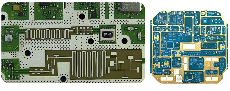
Key Design Factors in RF Microwave PCB Fabrication
Several fabrication parameters must be tightly controlled when manufacturing RF circuit boards.
Controlled impedance traces
RF signals travel through transmission lines that must maintain a specific impedance, commonly:
- 50Ω single-ended
- 100Ω differential
Small deviations can cause signal reflections.
Low-loss dielectric materials
High-frequency laminates reduce signal attenuation and improve stability across temperature and frequency ranges.
Surface finish selection
Surface finishes such as ENIG or ENEPIG are preferred for RF designs due to their flat surfaces and consistent conductivity.
Tight fabrication tolerances
RF PCBs typically require strict manufacturing tolerances for:
- Trace width
- dielectric thickness
- via positioning
These factors directly influence signal behavior at high frequencies.
RF Trace Width Calculator for Controlled Impedance
Transmission line impedance depends heavily on the width of the RF trace relative to the dielectric thickness.
The commonly used microstrip impedance formula is:
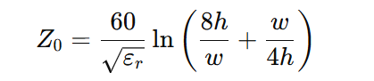
Where:
| Parameter | Description |
|---|---|
| Z0 | Characteristic impedance |
| εr | Dielectric constant |
| h | Dielectric thickness |
| w | Trace width |
Example
For a 50-ohm microstrip using Rogers RO4350B:
- dielectric constant ≈ 3.48
- dielectric thickness = 0.254 mm
Engineers calculate the required trace width and then fine-tune it during stack-up design.
In professional 5G RF PCB fabrication, manufacturers also run impedance simulations to verify the design before production.
Via Inductance Calculation in High-Frequency PCB Design
Vias connect layers inside multilayer PCBs, but at high frequencies they introduce parasitic inductance.
This inductance can distort signals and reduce RF performance.
The approximate via inductance can be calculated as:
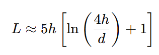
Where:
| Parameter | Description |
|---|---|
| L | Via inductance |
| h | PCB thickness |
| d | Via diameter |
Why it matters in RF fabrication
At microwave frequencies, even small inductances affect signal quality.
Design strategies often include:
- minimizing via length
- using via stitching
- reducing unused via stubs
Modern RF PCB fabrication may also include back drilling to remove via stubs that cause signal reflections.
Skin Effect Calculation for High-Frequency Conductors
At RF and microwave frequencies, current tends to flow only near the conductor surface. This phenomenon is called the skin effect.
Skin depth determines how deeply current penetrates into a conductor.
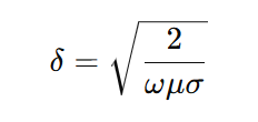
Where:
| Parameter | Description |
|---|---|
| δ | Skin depth |
| ω | Angular frequency |
| μ | Magnetic permeability |
| σ | Electrical conductivity |
Practical implication
At several gigahertz, current flows only through a thin copper layer.
This is why RF PCB fabrication often requires:
- smooth copper surfaces
- low-profile copper foil
- controlled copper roughness
Reducing conductor roughness helps minimize signal loss in high-frequency transmission lines.
Manufacturing Challenges in 5G RF Microwave PCB Fabrication
Producing high-frequency PCBs requires specialized manufacturing capabilities.
Material processing
High-frequency laminates behave differently from standard FR-4 during lamination and drilling.
Precision drilling
Microvias and RF grounding vias must be drilled with tight tolerances.
Surface flatness
Uneven surfaces can affect RF connectors and microwave components.
F testing
Manufacturers often perform impedance verification and signal integrity testing before delivery.
Choosing a Reliable High-Frequency PCB Manufacturer
Selecting an experienced fabrication partner is critical for successful RF designs.
A reliable manufacturer should provide:
- expertise with RF materials such as Rogers laminates
- precise impedance control capabilities
- RF stack-up engineering support
- small-batch prototype manufacturing
Working with a manufacturer familiar with RF and microwave circuits can significantly reduce development risks. Best Technology (EBest Circuit) is a professional PCB and PCBA manufacturer with extensive experience in RF, microwave, and high-frequency PCB fabrication for advanced communication systems. With over 20 years of industry expertise, our engineering team supports projects from high-frequency PCB design review and impedance control to precision PCB manufacturing and full PCBA assembly. We work with advanced materials such as Rogers and other low-loss laminates, ensuring stable performance for 5G, RF, and microwave applications. For reliable 5g ready RF microwave high-frequency PCB fabrication and PCBA services, contact our engineering team at sales@bestpcb.vn or +84-827-237566.
From an engineering perspective, 5G ready RF microwave high-frequency PCB fabrication requires a combination of advanced materials, precise manufacturing processes, and strong engineering knowledge. Unlike standard PCB production, high-frequency boards demand careful control of impedance, signal loss, and parasitic effects.
Understanding key calculations such as RF trace width, via inductance, and skin effect helps engineers design more reliable RF circuits while enabling manufacturers to fabricate boards that meet strict performance requirements. As wireless technologies continue to evolve, the demand for high-frequency PCB fabrication will only grow, making specialized manufacturing expertise increasingly important.
If you are developing RF, microwave, or 5G communication hardware and need a reliable partner for high-frequency PCB fabrication and PCBA assembly, our engineering team is ready to support your project from PCB manufacturing and component sourcing to full PCB assembly services. Feel free to contact us for technical consultation or a quotation at sales@bestpcb.vn or +84-827-237566.
FAQs About 5G Ready RF Microwave High-Frequency PCB Fabrication
What impedance values are typically used in 5G RF PCB designs?
Most RF and microwave circuits use 50Ω single-ended impedance or 100Ω differential impedance. Maintaining impedance tolerance within ±5% to ±10% is critical to prevent signal reflections and ensure stable RF performance.
What dielectric constant (Dk) is suitable for high-frequency PCBs?
High-frequency PCBs typically use materials with a dielectric constant between 2.2 and 3.5. Common laminates such as Rogers RO4350B (Dk≈3.48) or RT5880 (Dk≈2.2) provide stable electrical performance for 5G and microwave circuits.
How small can RF vias be in high-frequency PCB fabrication?
For RF and microwave boards, via diameters are often 0.2 mm to 0.3 mm. HDI designs may use microvias as small as 0.1 mm, which helps reduce parasitic inductance and improves signal integrity.
What copper thickness is recommended for high-frequency RF PCBs?
Most high-frequency PCBs use 0.5 oz to 1 oz copper (17–35 μm). Thinner copper can reduce conductor loss and improve signal performance at frequencies above several gigahertz.
What loss tangent is acceptable for microwave PCB materials?
For RF and microwave applications, materials typically have a loss tangent below 0.005. Ultra-low-loss laminates used in millimeter-wave systems may have tanδ below 0.001.
What frequency range defines microwave or high-frequency PCB applications?
High-frequency PCBs generally operate above 1 GHz, while microwave circuits typically cover 3 GHz to 30 GHz. Some advanced 5G and mmWave systems can operate at 24 GHz to 77 GHz or higher.