 language
Ceramic PCB Assembly
Ceramic printed circuit boards are no longer niche substrates reserved only for aerospace or military programs. As power density rises, thermal margins shrink, and reliability expectations tighten, ceramic PCB assembly has become a practical and often necessary solution for demanding electronic systems. Selecting the right ceramic PCB manufacturer is therefore a strategic decision, not a sourcing detail.
This guide explains what ceramic PCBs are, how they differ from conventional materials, where they are used, and what to expect from a qualified ceramic PCB assembly manufacturer in China.
What Is a Ceramic PCB?
A ceramic PCB is a printed circuit board that uses an inorganic ceramic material as the base substrate instead of organic laminates such as FR-4. Common ceramic substrates include alumina (Al₂O₃), aluminum nitride (AlN), and beryllium oxide (BeO).
Unlike glass-fiber laminates, ceramic substrates offer exceptional thermal conductivity, high dielectric strength, and mechanical stability across wide temperature ranges. These properties make ceramic PCBs particularly suitable for high-power, high-frequency, and harsh-environment electronics.
From an assembly perspective, ceramic PCBs behave very differently from standard boards. They dissipate heat rapidly, remain dimensionally stable during reflow, and support higher operating temperatures without degradation.
Features of Ceramic PCBs
Ceramic PCBs are selected not for convenience, but for performance advantages that organic materials cannot deliver.
Key features include:
- High thermal conductivity for efficient heat dissipation
- Excellent dielectric strength and low dielectric loss
- High operating temperature capability
- Minimal thermal expansion mismatch with semiconductor devices
- Strong chemical and moisture resistance
- Long-term reliability under thermal cycling
These characteristics directly translate into improved electrical stability, reduced failure risk, and extended product life in demanding applications.
Applications of Ceramic PCBs
Ceramic PCBs are widely used in sectors where heat, power, and reliability dominate design constraints.
Typical applications include:
- High-power LED lighting modules
- Power converters and inverters
- Automotive power electronics and EV systems
- RF and microwave communication devices
- Medical imaging and diagnostic equipment
- Aerospace and defense electronics
- Industrial laser drivers and motor control systems
In these applications, ceramic substrates often replace metal core PCBs or thick copper FR-4 when thermal limits are exceeded.
Ceramic PCB vs FR-4: What are Differences?
Ceramic PCBs and FR-4 boards serve very different design objectives.
FR-4 is optimized for cost, manufacturability, and general-purpose electronics. Ceramic PCBs are optimized for performance, stability, and thermal management.
In practical terms:
- Ceramic PCBs dissipate heat far more effectively than FR-4
- Ceramic substrates remain stable at temperatures that would degrade FR-4
- Dielectric properties of ceramics are more consistent at high frequencies
- FR-4 offers lower material and processing cost for standard designs
The choice is rarely about replacing FR-4 universally, but about selecting ceramic PCBs where FR-4 becomes a technical limitation.
Why Use Ceramic PCB Over Other PCBs?
Design teams choose ceramic PCBs when conventional substrates introduce unacceptable risks.
Common drivers include:
- Excessive junction temperatures in power devices
- Signal instability at high frequencies
- Warpage or delamination under thermal stress
- Long-term reliability requirements
- Compact designs with limited cooling options
In many cases, switching to ceramic PCBs simplifies thermal design, reduces the need for external heat sinks, and improves overall system robustness.
Best Technology – Your Trusted Ceramic PCB Assembly In China
From rapid ceramic PCB prototypes to stable volume production, Best Technology delivers end-to-end ceramic PCB assembly services tailored to your project scale and technical requirements. Our integrated manufacturing model ensures consistent quality, controlled lead times, and clear engineering accountability at every stage.
Our ceramic PCB assembly services include:
- SMT assembly
- Turnkey (full-service) assembly
- BGA and QFN assembly
- IC programming
- Through-hole assembly
- Mixed SMT & THT assembly
- Pin and connector assembly
- Ceramic circuit board assembly
- Component packaging support (Reels, Cut Tape, Tube, Tray, Loose Parts)
We source and purchase components from chip manufacturers worldwide, including Mouser, Digi-Key, Arrow Electronics, and other suppliers. Additionally, we maintain a substantial inventory of frequently used parts in our warehouse. When a particular component is unavailable, our engineers offer suggestions for suitable alternatives at reasonable prices.
Our Capabilities for Ceramic PCB Assembly
A qualified ceramic PCB assembly partner must address both material behavior and assembly precision.
Core capabilities should include:
- Expertise in alumina, AlN, and DBC ceramic substrates
- Substrate dimension: L5050MM~L510360MM
- Chip specification: 01005 packages and above parts
- BGA pitch: >=0.15mm with 100% 3D AOI and X-ray inspection
- Mount accuracy: 0.05mm
- Assembly speed: 0.04s/point
- Controlled solder paste selection for ceramic wetting behavior
- Optimized reflow profiles for high thermal conductivity boards
- Fine-pitch SMT and power device assembly
- AOI, X-ray inspection, and electrical testing
- Experience with low-CTE substrates and thick copper designs
Equally important is engineering support that understands ceramic PCB design constraints and can provide early DFM and DFA feedback.
Ceramic PCB Assembly Process – Detailed Guide
A successful ceramic PCB assembly process is not just about placing components; it is about managing heat flow, solder wetting behavior, and mechanical stress with precision.
Below is a step-by-step explanation of a professional ceramic PCB assembly process.
1. Incoming Material Inspection and Preparation
The process begins with strict incoming inspection of ceramic substrates and components.
Key inspection points include:
- Substrate type verification (Al₂O₃, AlN, DBC, etc.)
- Metallization quality (copper thickness, adhesion, surface finish)
- Flatness and micro-crack inspection
- Dimensional accuracy and pad geometry
Ceramic substrates are rigid and brittle. Any micro-defect introduced during fabrication or handling can propagate during thermal cycling. For this reason, ceramic PCBs are typically handled with dedicated fixtures and anti-shock packaging from the first step.
Surface preparation is also critical. Ceramic PCBs often require plasma cleaning or chemical cleaning to remove surface contaminants and improve solderability, especially for DBC and thick-copper designs.
2. Solder Paste Selection and Printing
Solder paste selection plays a decisive role in ceramic PCB assembly success.
Because ceramic substrates dissipate heat rapidly, the solder alloy must provide:
- Stable wetting behavior on ceramic-based metallization
- Good slump control to prevent bridging
- Compatibility with higher reflow peak temperatures
In many ceramic PCB assemblies, high-reliability solder alloys or silver-based pastes are selected, particularly for power devices and die-attach applications.
During solder paste printing:
- Stencil thickness is carefully matched to copper thickness and pad design
- Aperture reduction is often applied to prevent excess solder
- Printing pressure and speed are adjusted to avoid pad damage
Due to the hardness of ceramic substrates, alignment accuracy is more critical than with FR-4. Even minor stencil misalignment can lead to solder starvation or joint imbalance.
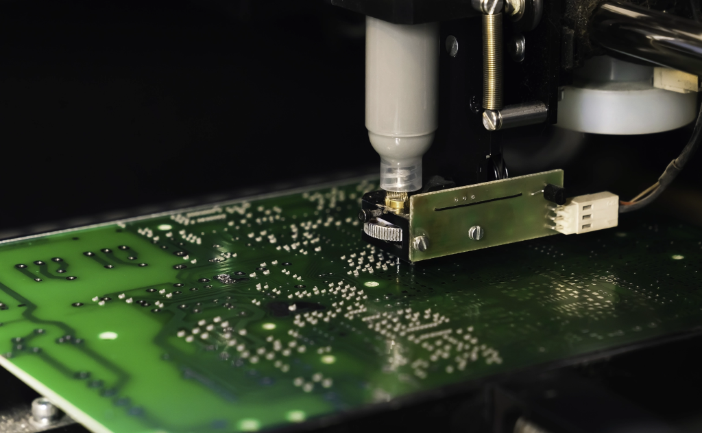
3. High-Precision Component Placement
Component placement on ceramic PCBs requires tighter control than conventional SMT.
Key considerations include:
- Placement force control to avoid cracking the substrate
- Accurate component centering to ensure uniform solder wetting
- Special handling for heavy power devices and large packages
Ceramic PCBs are unforgiving to mechanical stress. Advanced pick-and-place machines with controlled Z-axis force and vision alignment are typically used. For DBC ceramic PCBs, thick copper pads and large thermal masses demand extremely accurate placement to maintain solder joint symmetry.
4. Reflow Soldering with Optimized Thermal Profiles
Reflow soldering is the most critical stage in ceramic PCB assembly. A ceramic-specific reflow profile typically features:
- Slower ramp-up rates to protect components
- Extended soak zones to stabilize temperature gradients
- Higher peak temperatures to ensure full solder wetting
- Controlled cooling rates to reduce thermal stress
For aluminum nitride and DBC substrates, nitrogen reflow is often used to improve solder joint quality and reduce oxidation. Profile validation is usually performed using embedded thermocouples placed near critical components and high-current pads.
5. Special Processes for Power and Die-Attach Applications
Many ceramic PCB assemblies involve power semiconductors, bare dies, or large thermal pads.
Additional processes may include:
- Sintered silver bonding for high-power devices
- High-temperature soldering for multi-step assemblies
- Controlled pressure bonding for die attach
- Post-reflow stress relief cycles
These steps require dedicated equipment and experienced process engineers, as improper control can lead to voiding, delamination, or premature failure under thermal cycling.
6. Optical and X-Ray Inspection
Inspection on ceramic PCBs goes beyond standard AOI.
AOI focuses on:
- Solder joint shape and wetting quality
- Component alignment and polarity
- Surface defects and solder bridging
X-ray inspection is especially important for:
- Bottom-terminated components
- Thick copper and DBC ceramic PCBs
- Power modules with large thermal pads
X-ray analysis helps detect voids, insufficient solder fill, and hidden defects that cannot be identified optically but directly impact thermal and electrical performance.
7. Electrical Testing and Functional Verification
After assembly, ceramic PCBs undergo electrical and functional testing appropriate to their application.
Testing may include:
- Continuity and isolation testing
- High-voltage withstand testing
- Functional power-on testing
- Thermal performance validation
Because ceramic PCBs are often used in mission-critical systems, test coverage is typically higher than for standard assemblies.
8. Final Cleaning, Packaging, and Reliability Control
Flux residues on ceramic PCBs can compromise insulation resistance and long-term reliability.
Final steps usually include:
- Precision cleaning with validated solvents
- Ionic contamination testing when required
- Visual inspection under magnification
- Shock-resistant packaging to protect brittle substrates
For automotive, medical, or industrial applications, ceramic PCB assemblies may also undergo burn-in, thermal cycling, or accelerated life testing.
If your project involves high power density, elevated operating temperatures, or long-term reliability requirements, ceramic PCB assembly may be the most effective solution.
Partnering with an experienced ceramic PCB assembly manufacturer ensures that material advantages translate into real-world performance, yield stability, and product longevity.
For technical consultation, design review, or ceramic PCB assembly quotations, engage with a manufacturer that understands both the material science and the assembly discipline behind ceramic PCBs.