 language
Common 13 Types of Soldering Defects in PCB Assembly
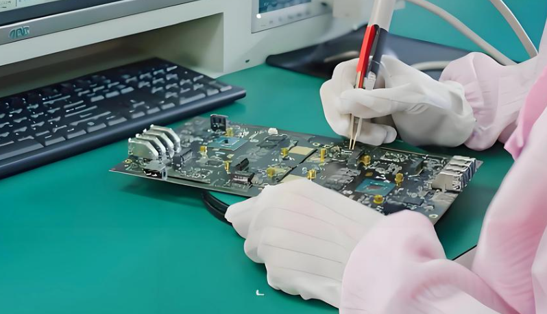
Soldering is one of the most critical steps in PCB assembly (PCBA). A reliable solder joint ensures strong electrical connectivity and mechanical stability between the component lead and the PCB pad. However, during SMT reflow or wave soldering, several defects may appear due to improper temperature profiles, poor material quality, design issues, or process deviations.
Understanding these soldering defects helps engineers improve yield, reduce rework, and ensure product reliability.
Types of Soldering Defects
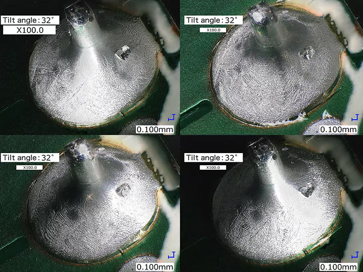
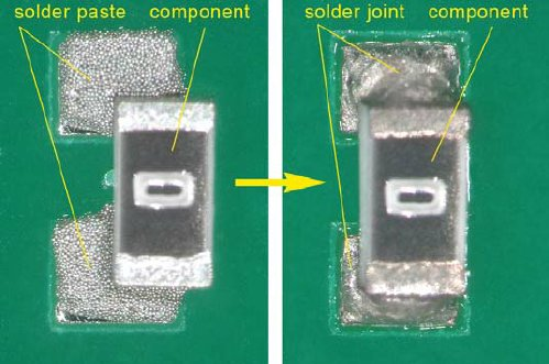
What Is a Good PCB Solder Joint?
Before discussing soldering defects, it is important to understand the characteristics of a high-quality solder joint. A good solder joint should have the following features:
- Smooth and shiny surface appearance
- Proper wetting between solder, pad, and component lead
- Concave solder fillet shape
- No cracks, voids, or contamination
- Adequate mechanical strength
In SMT assembly, achieving these characteristics requires careful control of solder paste printing, component placement, and reflow temperature profiles.
1. Cold Solder Joint
A cold solder joint occurs when the solder does not fully melt or properly bond with the pad and component lead. Instead of forming a smooth metallurgical bond, the solder solidifies prematurely, resulting in a weak electrical and mechanical connection.
Cold joints are typically identified by their dull, rough, or grainy appearance. Unlike a good solder joint that has a shiny and smooth surface, cold joints often look uneven or cracked.
Precautions
- Optimize reflow soldering temperature profile
- Ensure proper flux activity
- Avoid board vibration during cooling
- Use fresh components and clean pads
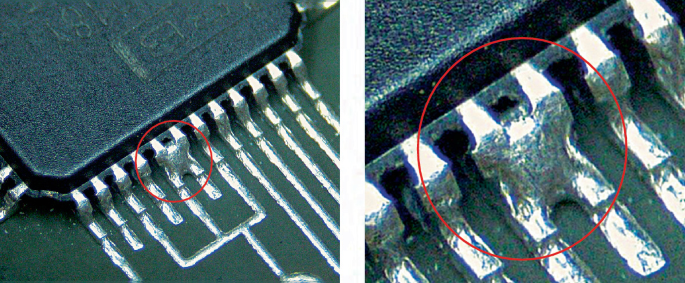
2. Solder Bridge
A solder bridge occurs when solder unintentionally connects two adjacent pads or component leads. This defect forms a conductive path that can create short circuits between signals.
Solder bridging is especially common in fine-pitch components such as:
- QFP packages
- QFN devices
- BGA pads
- Small pitch connectors
Precautions
- Optimize stencil aperture size
- Maintain correct solder paste volume
- Improve pick-and-place accuracy
- Use proper solder mask spacing
3. Tombstoning (Manhattan Effect)
Tombstoning occurs when a chip component lifts vertically during reflow, leaving one end soldered while the other rises upward. This defect resembles a tombstone or standing monument, which is why it is called the Manhattan effect.
It commonly affects small passive components such as:
- 0201 resistors
- 0402 capacitors
- small inductors
Precautions
- Ensure symmetrical pad design
- Maintain consistent paste deposition
- Balance heating during reflow
- Use proper PCB layout rules
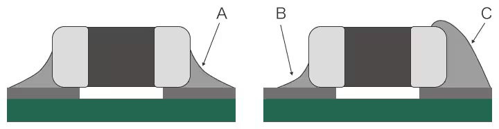
4. Insufficient Solder
Insufficient solder means that too little solder forms on the joint, resulting in a weak mechanical and electrical connection. In many cases, the solder fillet is small, or the pad surface remains partially exposed.
Common Causes
- Small stencil aperture
- Low solder paste deposition
- Improper printing pressure
- Oxidized pads
Precautions
- Adjust stencil thickness and aperture design
- Improve solder paste printing process
- Inspect paste deposition using SPI (Solder Paste Inspection)
5. Excessive Solder
Excess solder forms large solder blobs or overly large fillets around component leads. Although the joint may still function electrically, excessive solder often causes reliability concerns.
Common Causes
- Large stencil openings
- Excess solder paste
- Low viscosity solder paste
Precautions
- Optimize stencil design
- Control paste printing volume
- Maintain proper paste storage conditions
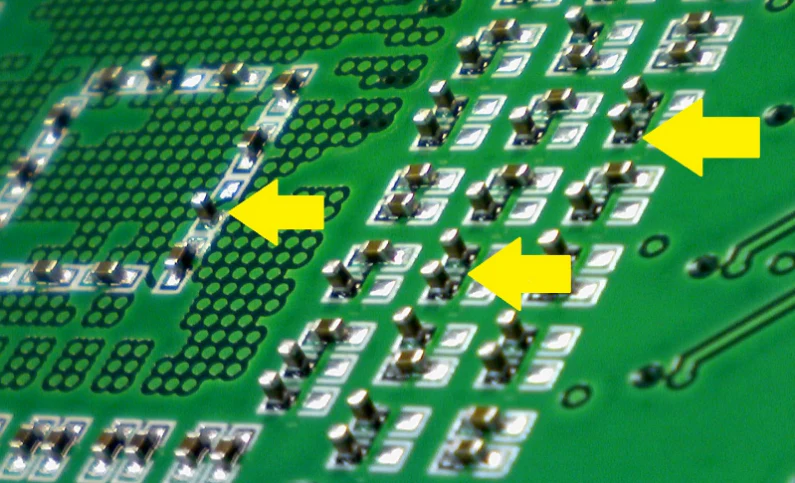
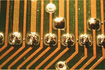
6. Solder Balling
Solder balling refers to the formation of many small spherical solder particles around the solder joint after the reflow process. These solder balls may remain attached to the PCB surface, trapped under components, or loosely scattered around pads.
Unlike a normal solder joint that forms a smooth fillet, solder balling creates separate tiny solder beads that are not properly bonded to the pad. The diameter of these solder balls can range from tens of microns to several hundred microns. In many cases, solder balls appear around chip resistors, capacitors, QFN devices, or BGA components.
Precautions
- Bake moisture-sensitive PCBs/components
- Optimize reflow temperature ramp rate
- Use high-quality solder paste
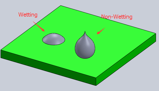
7. Non-Wetting
Non-wetting occurs when molten solder fails to properly spread across the PCB pad or component lead during soldering. Instead of forming a uniform metallurgical bond, the solder gathers into irregular shapes or beads.
A typical non-wetting joint leaves large portions of the copper pad exposed, indicating poor solder adhesion.
Precautions
- Clean PCB surfaces
- Use fresh solder paste
- Store PCBs properly to prevent oxidation
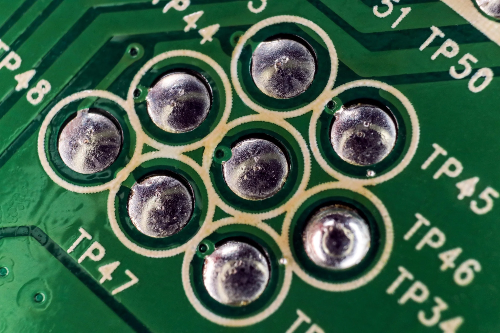
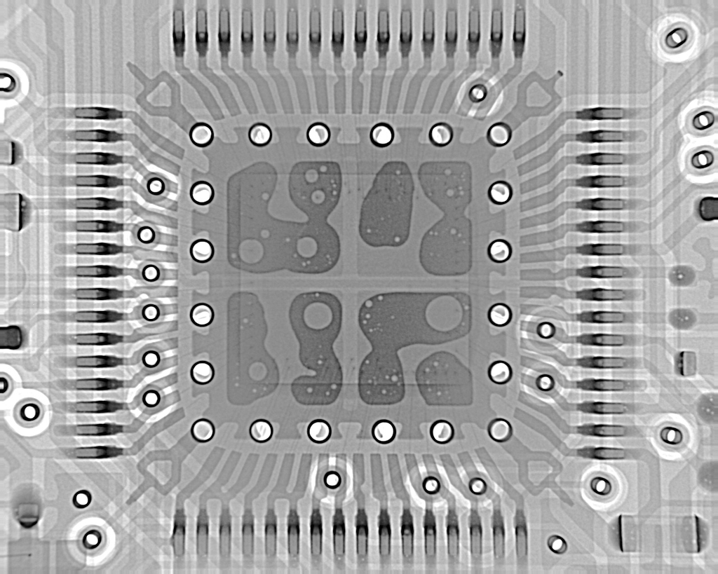
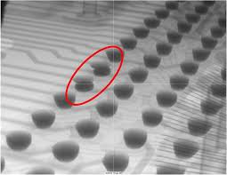
8. Solder Voids
Solder voids are internal air pockets trapped inside a solder joint. These voids are invisible to the naked eye and are typically detected using X-ray inspection systems. Voiding frequently occurs in components that have large thermal pads, such as:
- BGA packages
- QFN devices
- Power MOSFET packages
- LED thermal pads
Void sizes may vary from small micro-voids to large cavities that occupy over 20–30% of the solder joint area.
Precautions
- Optimize reflow profile
- Improve PCB surface finish quality
- Use vacuum reflow when necessary
9. Component Misalignment
Component misalignment occurs when a component is shifted from its intended position on the PCB pad after placement or reflow soldering.
This defect is commonly seen as:
- Skewed chip resistors
- Rotated IC packages
- Offset connectors
The misalignment may be slight or severe enough that the component partially misses the solder pad.
Precautions
- Calibrate placement machines
- Maintain consistent solder paste printing
- Follow IPC pad design guidelines
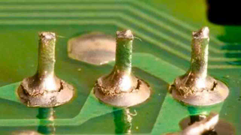
10. Lifted Pads
A lifted pad occurs when the copper pad separates from the PCB substrate. Instead of remaining bonded to the laminate, the pad lifts upward, often attached to the component lead. This defect usually appears after manual rework, excessive heating, or mechanical stress.
Precautions
- Control soldering temperature
- Reduce repeated rework cycles
- Use high-quality PCB materials
11. Solder Cracking
Solder cracking refers to the formation of microfractures or visible cracks inside a solder joint. These cracks usually develop over time due to mechanical or thermal stress. Cracks are commonly found in:
- BGA joints
- large connectors
- power components
Precautions
- Use appropriate solder alloys
- Design for thermal stress relief
- Add mechanical reinforcement if needed
12. Head-in-Pillow Defect
Head-in-pillow (HIP) is a specific defect in BGA assembly where the solder ball and solder paste melt but fail to merge into a single joint. The result is a solder ball resting on top of the paste like a pillow.
Precautions
- Optimize reflow thermal profile
- Improve PCB flatness
- Use advanced X-ray inspection
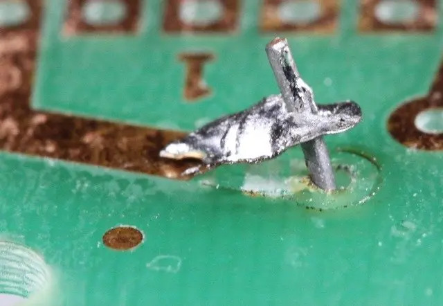
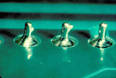
13. Solder Icicles
Solder icicles are sharp, needle-like projections of solder that form during the wave soldering process.
When the PCB leaves the molten solder wave, excess solder should drain back into the solder bath. If the withdrawal speed or angle is incorrect, molten solder stretches and solidifies into spikes.
Precautions
- Adjust wave solder parameters
- Optimize conveyor speed
- Maintain correct solder temperature
Why Process Control Is Critical in PCB Assembly?
Preventing solder defects requires strict control of the entire PCB assembly process, including:
- Solder paste printing
- Component placement accuracy
- Reflow temperature profile
- PCB material quality
- Environmental humidity control
Professional PCBA manufacturers typically implement multiple inspection steps:
- SPI (Solder Paste Inspection)
- AOI (Automated Optical Inspection)
- X-ray inspection
- Functional testing
These technologies ensure that solder defects are detected early and corrected before final product shipment.
Why Choose Best Technology for Reliable PCB Assembly?
At Best Technology, we focus on engineering collaboration, stable manufacturing processes, and responsive technical support to help customers move from design to production with confidence.
We have over 19 years experiences in PCB assembly with over 3000m2 factory in Shenzhen city. To serve customer better, we have setup a SMT factory in Vietnam to support oversea orders with fast delivery and more competitive price.
Key advantages of working with Best Technology include:
- Full turnkey service from PCB design to PCB assembly
- Components sourcing service support & strong supply chain network
- Fast delivery with 1.5 weeks
- Support small batch and mass production
- DFM review & BOM optimization
- Digital manufacturing & traceability
- Full entire set of testing equipment
- ISO9001, ISO13485, IATF16949, and AS9100D certificated
Today, Best Technology has supported 10,000+ engineers and over 1,800 customers worldwide, delivering reliable PCB and PCBA solutions for industries such as medical devices, automotive electronics, industrial control systems, and communication equipment.
If you are looking for a reliable PCB assembly partner for your next project, our engineering team is ready to assist. Contact us: sales@bestpcb.vn