 language
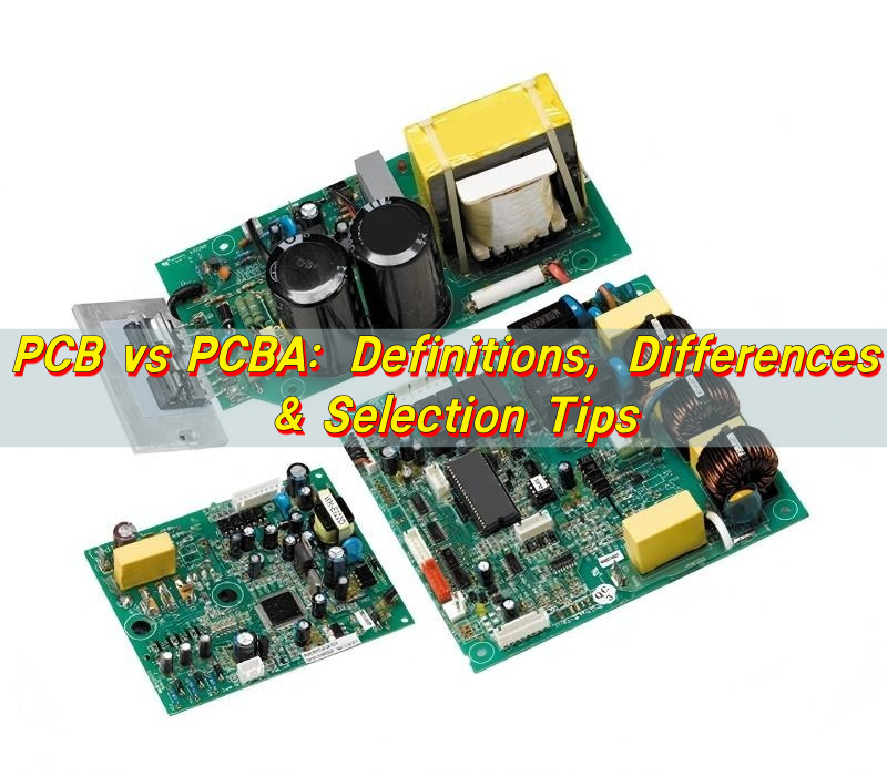
PCB vs PCBA: Definitions, Differences & Selection Tips
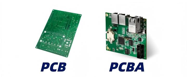
Modern electronics rely on a strong foundation that supports every chip, connector, and circuit. That foundation is the printed circuit board and the assembled circuit board. In simple terms, a PCB refers to the bare board that provides the physical platform and electrical pathways for electronic components. PCBA refers to that same board after components are mounted and soldered. The difference may sound straightforward, but the design, manufacturing flow, cost structure, and application scenarios behind each stage are quite different.
For companies that develop electronic devices, learning how these stages connect within the production chain helps avoid delays and improves product quality. Manufacturers like Best Technology Co., Ltd., which has specialized in PCB fabrication and electronic assembly for many years, typically provide both fabrication and assembly services. This integrated capability simplifies supply chain management and ensures consistent quality across the entire manufacturing process.
What is a PCB?
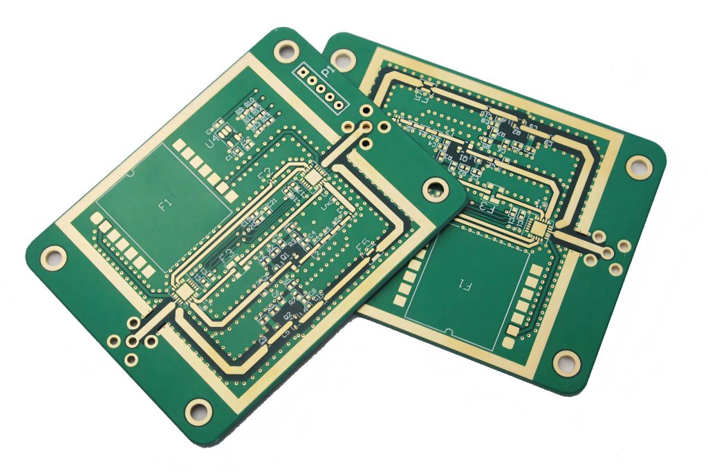
A printed circuit board, commonly called a PCB, is the structural base of most electronic devices. It is a flat board made of insulating material with conductive copper pathways that connect different electronic components. These copper traces act like roads that allow electrical signals to travel between parts of a circuit.
Before any components are installed, the board itself already contains a carefully designed pattern of conductive tracks. Engineers design these patterns using specialized layout software, ensuring signals travel correctly and electrical interference stays under control.
Most boards consist of several layers of material bonded together. The core is usually fiberglass reinforced epoxy, often called FR-4. Copper foil layers sit on top of the core and form the conductive paths. Protective coatings and markings are added later to improve durability and readability.
The role of the PCB is simple yet essential. It supports electronic parts physically and ensures signals flow correctly between them. Without this structured platform, complex circuits would require many loose wires, which would be unreliable and difficult to maintain.
Printed circuit boards appear in almost every electronic product used today. Smartphones, computers, automotive control systems, and industrial equipment all depend on reliable board designs.
Some common characteristics of PCBs include:
- A rigid or flexible insulating substrate
- Copper traces that carry electrical signals
- Mounting holes and pads for components
- Protective solder mask layers
- Silkscreen markings for identification
PCBs come in several structural types. Each type serves different design requirements and performance levels.
Common PCB types include:
- Single-layer boards used for simple electronics
- Double-layer boards that allow more routing flexibility
- Multilayer boards with several internal layers for high-density circuits
- Rigid-flex boards combining flexible and rigid sections
- High-frequency boards designed for RF applications
During fabrication, manufacturers follow a precise sequence of processes. Each step ensures electrical accuracy and structural stability.
Typical PCB manufacturing steps include:
- Circuit design and layout preparation
- Raw material preparation and copper lamination
- Image transfer and copper etching
- Drilling and hole plating
- Solder mask coating and curing
- Silkscreen printing and surface finishing
- Electrical testing and final inspection
A well-designed PCB forms the backbone of an electronic device. When the fabrication quality is high, assembly becomes more reliable and long-term performance improves significantly.
What is a PCBA?
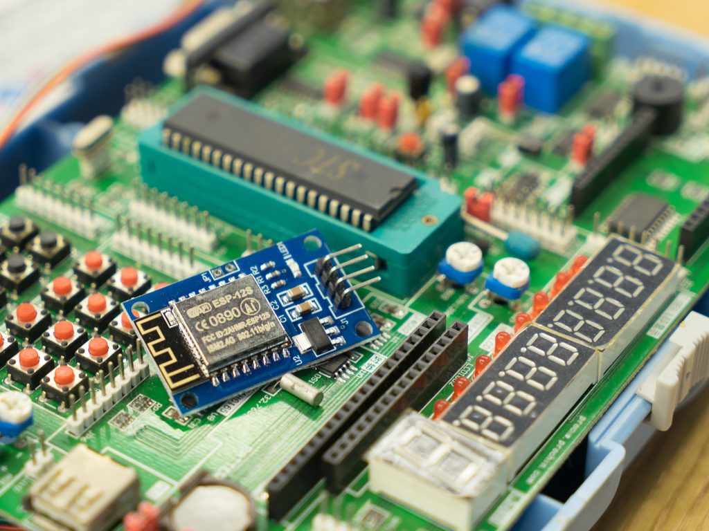
PCBA stands for printed circuit board assembly. This term refers to the board after electronic components have been mounted and soldered onto it. Once assembly is complete, the board becomes a functional electronic module capable of performing its designed tasks.
At the PCBA stage, the bare board transforms into a working circuit. Components such as resistors, capacitors, integrated circuits, connectors, and sensors are attached to specific pads on the board. Assembly machines or technicians then secure them using solder.
Several technologies exist for component placement. Surface mount technology is the most common method today. Components are placed directly onto the surface of the board and soldered using automated equipment. This approach supports high production speed and compact circuit design.
Another method is through-hole technology, where component leads pass through holes drilled in the board. These leads are soldered on the opposite side. This technique provides strong mechanical bonding and remains useful for connectors or large components.
A typical assembly line combines advanced machines with strict quality inspection. This ensures components are placed accurately and solder joints remain reliable.
Common assembly steps include:
- Applying solder paste to component pads
- Automated component placement using pick-and-place machines
- Reflow soldering to melt solder and create electrical connections
- Optical inspection to verify component alignment
- Functional testing to ensure correct operation
Once the board passes inspection, it can be integrated into a larger electronic product. Some boards are installed directly into devices, while others become sub-assemblies within complex systems. Many electronics manufacturers prefer working with companies that provide both PCB fabrication and assembly services. This approach improves coordination between design, manufacturing, and testing.
Best Technology Co., Ltd., for example, offers integrated solutions that combine board fabrication with advanced SMT assembly lines. Their facilities in Asia support a wide range of industries including consumer electronics, automotive electronics, industrial control systems, and communication equipment.
What is the difference between PCB and PCBA?
The distinction between PCB and PCBA lies mainly in their stage within the electronics manufacturing process. One represents the board before components are installed, while the other represents the completed electronic assembly.
A PCB is simply the structural platform that carries electrical pathways. It contains no active or passive components. The board itself cannot perform electronic functions until parts are added.
A PCBA, in contrast, includes all electronic components mounted onto the board and connected through solder joints. Once assembly is complete, the board can process signals, manage power, or perform control functions depending on the circuit design.
When someone orders PCBs, they are requesting only the fabricated boards. When they request PCBA services, they expect component sourcing, assembly, and testing as well. The relationship between the two is similar to that of a chassis and a finished machine. The chassis forms the structure, while the completed machine includes all operating parts.
The table below highlights the main distinctions between these two terms.
| Feature | PCB | PCBA |
|---|---|---|
| Definition | Bare printed circuit board without components | Fully assembled circuit board with components |
| Function | Provides mechanical support and electrical pathways | Performs electronic functions |
| Manufacturing stage | Fabrication stage | Assembly stage |
| Components | None installed | Resistors, capacitors, ICs and other parts mounted |
| Testing | Electrical continuity testing | Functional and performance testing |
| Cost structure | Lower cost due to material and fabrication only | Higher cost including components and assembly |
PCB vs PCBA: What does each stand for?
PCB stands for Printed Circuit Board. The term describes a board that contains conductive tracks printed onto an insulating substrate. These tracks connect electronic components and allow electrical signals to flow between them.
PCBA stands for Printed Circuit Board Assembly. This phrase refers to the process and result of mounting components onto the board. It also describes the finished board after assembly is complete.
Although the two acronyms share the same base structure, the extra letter “A” in PCBA highlights the assembly stage. This single letter represents the entire process of component placement, soldering, inspection, and testing.
For example:
- Ordering PCB fabrication means requesting only the bare boards.
- Ordering PCBA services includes component sourcing and assembly.
- Requesting turnkey assembly often includes both fabrication and assembly.
Many contract manufacturers provide turnkey services because it simplifies project management for clients. Instead of coordinating several vendors, customers work with a single supplier responsible for the complete manufacturing process. Best Technology is one example of a manufacturer that offers both fabrication and assembly capabilities. This integrated service allows design teams to move smoothly from board layout to final electronic module production.
How to tell PCB apart from PCBA?
A bare board has a clean appearance with visible copper patterns and protective coatings, while an assembled board contains many mounted components. Here are simple ways to distinguish them:
- Component presence
A PCB has no components attached. A PCBA contains chips, capacitors, resistors, connectors, and other parts. - Surface complexity
Bare boards appear flat and uniform. Assembled boards have many components with varying shapes and heights. - Solder joints
PCBA boards show shiny solder connections where components attach to pads. - Testing labels
Assembled boards often include inspection markings or serial labels.
In professional manufacturing environments, additional inspection tools help verify the assembly stage. Automated optical inspection systems check component alignment and solder quality. X-ray inspection may also be used for hidden solder joints such as those under BGA packages.
Another useful difference relates to electrical functionality. A PCB cannot perform any electronic function by itself. Once the board becomes a PCBA, it can be powered and tested within a working circuit.
What is the cost difference between PCB and PCBA?
The price difference between a PCB and a PCBA can be significant because they represent different manufacturing stages. Several factors influence the overall cost difference.
A PCB includes the cost of raw materials, fabrication processes, and quality inspection. The materials typically include copper foil, laminate substrates, solder mask, and surface finishes. Manufacturing steps such as drilling, plating, and etching contribute to production cost.
PCBA costs include everything required to build the functional board. This means the price includes the fabricated board, electronic components, assembly labor, machine operation, and testing procedures.
Key cost factors include:
- Board complexity and layer count
- Number and type of electronic components
- Assembly technology such as SMT or through-hole
- Testing requirements and quality standards
- Production volume
| Cost Category | PCB | PCBA |
|---|---|---|
| Raw materials | Substrate, copper foil | PCB materials plus electronic components |
| Manufacturing processes | Fabrication steps only | Fabrication plus assembly |
| Equipment use | Fabrication equipment | SMT lines, reflow ovens, inspection systems |
| Labor requirements | Fabrication technicians | Assembly operators and testing engineers |
| Testing scope | Electrical continuity | Functional and reliability testing |
In most cases, the cost of components forms the largest portion of the PCBA price. Complex integrated circuits or specialized sensors can significantly increase the overall assembly cost.
Working with experienced manufacturers helps manage these expenses effectively. Companies such as Best Technology often assist customers with design optimization, component sourcing, and manufacturing planning. These services can reduce overall production cost while maintaining high reliability.
What is the production process for PCB vs PCBA?
The production workflow for electronic boards usually occurs in two major phases. The first phase focuses on board fabrication, while the second phase involves assembly and testing. The fabrication stage converts raw laminate materials into structured circuit boards. The assembly stage transforms those boards into functional electronic modules.
PCB fabrication process: The fabrication process begins with circuit design data generated by engineers. This design data defines copper trace patterns, drilling locations, and board dimensions.
Key fabrication steps typically include:
- Design verification
Engineers review layout data to confirm manufacturability. - Material preparation
Copper-clad laminates are cut to the required panel size. - Imaging and etching
The circuit pattern is transferred to copper layers and unwanted copper is removed. - Drilling and plating
Holes are drilled and plated with copper to create electrical connections between layers. - Solder mask application
A protective coating covers the board surface except for exposed pads. - Silkscreen printing
Labels and component markings are printed on the board. - Electrical testing
Automated equipment verifies circuit continuity.
PCBA assembly process: After the bare boards pass inspection, they move to the assembly line. At this stage components are installed according to the design specifications.
Typical assembly steps include:
- Solder paste printing on component pads
- High-speed component placement using automated machines
- Reflow soldering to form permanent electrical connections
- Optical inspection to detect alignment issues
- Functional testing and quality verification
Advanced assembly lines can place tens of thousands of components per hour. This high level of automation ensures consistency and efficiency in modern electronics manufacturing. Manufacturers like Best Technology combine fabrication facilities with SMT assembly lines. This integrated structure reduces production lead time and improves communication between fabrication and assembly teams.
What are the applications of PCB and PCBA?
Printed circuit boards and assembled boards appear in almost every modern electronic device. From everyday consumer gadgets to complex industrial systems, these technologies provide the foundation for electronic functionality.
A bare board itself does not perform electronic operations, but it forms the base that allows circuits to exist in a compact and reliable structure. Once assembled with components, the board becomes the central control platform of many devices.
Common application areas include:
- Consumer electronics
Smartphones, tablets, wearable devices, and home appliances rely on compact boards to manage processing, power, and communication. - Industrial automation
Control systems, sensors, and monitoring equipment depend on durable circuit assemblies for reliable operation. - Automotive electronics
Engine control units, infotainment systems, and safety modules use advanced board assemblies designed for harsh environments. - Medical equipment
Diagnostic machines and monitoring devices require high-precision electronic assemblies to ensure accuracy and reliability. - Communication systems
Network routers, signal transmitters, and base station equipment use multilayer boards for high-speed signal transmission.
Manufacturers with strong design support and production capability can help clients adapt to these trends. Best Technology, for example, supports customers across several industries by providing reliable PCB fabrication and PCBA services that meet international quality standards.
FAQ
What is the main difference between PCB and PCBA?
The primary difference lies in the manufacturing stage. A PCB is the bare board with conductive pathways but no components installed. A PCBA is the completed assembly where electronic components are mounted and soldered onto the board, allowing it to function as part of an electronic system.
Can a PCB work without assembly?
A PCB alone cannot perform electronic tasks because it lacks components such as integrated circuits and resistors. Once the board undergoes assembly and becomes a PCBA, it can operate within an electronic device.
Which process comes first, PCB fabrication or PCBA assembly?
PCB fabrication always occurs first. The bare board must be produced before components can be mounted. After fabrication, the boards move to assembly lines where electronic components are installed and tested.
Why do many companies prefer turnkey PCB assembly services?
Turnkey services allow one supplier to manage board fabrication, component sourcing, assembly, and testing. This reduces communication delays, improves coordination, and simplifies project management for product developers.
Are PCB and PCBA used in the same products?
Yes. The final product usually contains assembled boards. The PCB stage occurs earlier during manufacturing, while the PCBA stage represents the finished electronic module integrated into the device.
Conclusion:
Companies that combine fabrication and assembly capabilities offer valuable advantages for product developers. Integrated manufacturing reduces supply chain complexity, shortens production cycles, and improves quality consistency.
Best Technology Co., Ltd. has extensive experience in PCB manufacturing and electronic assembly services, helping customers transform innovative designs into reliable products. Their facilities support a wide range of industries and follow strict quality standards to ensure dependable results.
If you would like to learn more about PCB fabrication or PCBA assembly solutions, feel free to contact the professional team at sales@bestpcb.vn