 language
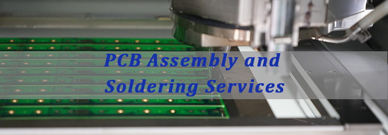
PCB Assembly and Soldering Services | Free DFM
PCB Assembly and Soldering Services transform a bare printed circuit board into a functional electronic unit, integrating components through precise processes to bring your design to life. This comprehensive guide delves into the intricacies of PCBA, explains various soldering techniques, highlights common pitfalls, and outlines how to ensure top-tier quality for your projects.
Are you experiencing these problems during PCB assembly and soldering?
| Common Challenges | Our Solutions |
|---|---|
| Hidden solder defects such as cold joints or tombstoning | Free DFM review before production |
| Unexpected delays or cost overruns | Engineering review and BOM optimization |
| Poor solder joint reliability | Strict process control and certified materials |
| Defects in BGA or fine-pitch components | AOI and X-ray inspection |
| Managing multiple suppliers for PCB and assembly | One-stop PCB + PCBA service |
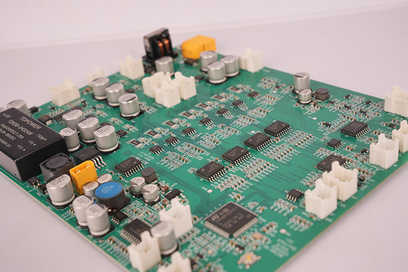
At Best Technology, we are a professional PCB assembly and soldering services provider with our own PCB and PCBA manufacturing facilities. Our capabilities cover SMT assembly, through-hole assembly, soldering, testing, and full PCBA production, giving customers a more efficient and reliable path from design to delivery. Because we operate both PCB and PCBA factories in-house, we can manage quality, lead time, and process coordination more effectively. Our team also provides a free DFM review before production to help engineers improve manufacturability, reduce assembly risks, and move projects forward with greater certainty. Whether you need prototype support or mass production, we deliver one-stop PCB + PCBA services backed by responsive engineering support. To discuss your project, just feel free to contact us at sales@bestpcb.vn.
What Are PCB Assembly and Soldering Services?
PCB Assembly (PCBA) and soldering are the core processes in electronics manufacturing where components are permanently attached to a printed circuit board to create a functional assembly. While often used interchangeably, soldering is a critical sub-process within the broader assembly workflow. This section clarifies their definitions, interrelationship, and ultimate importance in product creation.
- PCB Assembly (PCBA): The Macro Process. This is the complete sequence of steps to populate a PCB. It encompasses solder paste application, component placement, soldering, cleaning, and inspection. The goal is to produce a fully operational circuit board assembly.
- Soldering: The Micro Connection. Soldering is the specific metallurgical process of joining component leads to PCB pads using a molten alloy (solder). It forms both the electrical and mechanical bond. The quality of soldering directly dictates the assembly’s reliability.
- The Relationship. Think of PCBA as building a house, and soldering as the act of welding the steel frame or securing the bricks. One cannot exist without the other for creating a stable structure. High-quality PCB Assembly and Soldering Services are inseparable.
- Critical Importance. Robust soldering ensures signal integrity, power delivery, and long-term durability. Poor soldering is the leading cause of field failures, including intermittent connections, thermal breakdown, and open circuits.
In essence, PCB Assembly and Soldering Services are the fundamental bridge between a theoretical design and a tangible, working electronic product, with soldering quality being the linchpin of its long-term success.
What Is the Difference Between PCB Assembly and PCB Soldering?
Understanding the difference between PCB assembly and PCB soldering helps engineers communicate more clearly with manufacturers and choose the right production service. Although the two terms are closely related, they represent different stages of the electronics manufacturing process.
| Aspect | PCB Assembly (PCBA) | PCB Soldering |
|---|---|---|
| Scope | Complete board assembly | One assembly step |
| Goal | Build a functional PCB | Create solder joints |
| Key Activities | Placement, soldering, testing | Reflow / wave / selective soldering |
| Process Stage | Full manufacturing workflow | After component placement |
| Result | Fully assembled PCB | Electrical connections |
Understanding the Two Processes
PCB Assembly (PCBA) refers to the entire manufacturing process of turning a bare printed circuit board into a working electronic unit. It typically includes solder paste printing, component placement, soldering, cleaning, inspection, and electrical testing.
PCB Soldering, on the other hand, is a specific manufacturing step within the assembly process. During this stage, solder alloy is melted to create electrical and mechanical connections between component leads and PCB pads. Common soldering methods include reflow soldering, wave soldering, and selective soldering.
In simple terms, PCB soldering is one operation within the broader PCB assembly workflow. When companies outsource PCB assembly and soldering services, they are typically looking for a manufacturer that can manage the entire production process—from component placement to soldering and final testing—before delivering a fully assembled PCB ready for integration.
What Types of PCB Soldering Processes Are Used in PCBA?
Choosing the correct soldering process is pivotal for quality, cost, and suitability. Modern PCB Assembly and Soldering Services employ several key techniques, each ideal for different component types and board designs.
- Reflow Soldering: The standard for Surface Mount Technology (SMT). Solder paste is printed on pads, components are placed, and the entire board passes through a reflow oven with precisely controlled temperature zones, melting the paste to form joints.
- Wave Soldering: Traditionally used for Through-Hole Technology (THT). The bottom side of the board passes over a wave of molten solder, which wicks up into the plated-through holes to solder the component leads.
- Selective Soldering: An advanced process where a mini wave or solder jet targets specific through-hole components on an otherwise SMT-assembled board, protecting sensitive SMDs from excess heat.
- Hand Soldering: Used for rework, prototyping, or attaching delicate, odd-form components that cannot withstand automated processes. Requires highly skilled technicians.
- Vapor Phase Soldering: Uses a saturated vapor of a heating fluid to provide uniform, precise heating. Excellent for complex boards with low thermal mass components or where temperature sensitivity is a concern.
The selection among these PCB soldering processes is a strategic decision based on your Bill of Materials (BOM) and design, directly impacting the PCB assembly production time and final quality.
How Does PCB Assembly and Soldering Work?
A reliable PCBA service follows a meticulous, multi-stage pipeline. Here’s a step-by-step breakdown of a typical SMT-dominated assembly workflow, which underscores the importance of integrated PCB Assembly and Soldering Services.
- Step 1: Design Review & DFM (Pre-Production). The most critical phase. Our Free DFM analysis checks for footprint errors, spacing issues, thermal imbalances, and other factors affecting solderability and yield.
- Step 2: Solder Paste Application. Solder paste (a mix of tiny solder spheres and flux) is precisely stenciled onto the PCB pads where SMDs will sit.
- Step 3: Component Placement. High-speed pick-and-place machines accurately position SMD components onto the pasted pads. For THT parts, this may be manual or automated insertion.
- Step 4: Soldering.
- For SMDs: The board enters a reflow soldering oven. The paste melts, forms joints, and then cools solidifying the connection.
- For THTs: The board undergoes wave soldering or selective soldering.
- Step 5: Cleaning & Inspection. Flux residue is cleaned. Boards then pass through Automated Optical Inspection (AOI) for surface defects and X-ray for hidden issues like BGA soldering voids.
- Step 6: Testing & Final Assembly. Functional testing (ICT, FCT) validates performance. Any through-hole or final components are added, followed by final QC.
This streamlined, quality-gated process ensures that every board meets specification, demonstrating how professional PCB Assembly and Soldering Services work in concert to deliver reliability.
What Is Through-Hole PCB Assembly and When Is It Used?
Through-Hole Technology (THT) assembly involves inserting component leads through drilled holes in the PCB and soldering them on the opposite side. While largely supplanted by SMT for miniaturization, THT remains indispensable for specific applications.
- High Mechanical Stress: Components like connectors, large transformers, or devices in automotive/vibration-prone environments benefit from THT’s superior mechanical bond.
- High Power/High Voltage: Components handling significant power or voltage often have larger leads, suited for robust through-hole connections.
- Prototyping & Manual Adjustment: THT components are easier to manually insert, solder, and replace, making them ideal for prototyping, test points, or adjustable parts (e.g., potentiometers).
- Exceptional Reliability: The through-board connection is extremely robust, often specified in aerospace, military, and critical industrial equipment where failure is not an option.
Finally, the choice between SMT and THT assembly isn’t always either/or. Many modern boards use a mixed-technology approach: SMT for the majority of components for density and speed, and THT for the specific parts listed above. This highlights the need for a PCB Assembly and Soldering Services provider proficient in both wave/reflow and selective soldering.
What Are the Most Common PCB Soldering Defects?
Even with automated production lines, soldering defects can still occur during PCB assembly. Understanding common soldering defects helps engineers identify process problems early and improve manufacturing reliability.
| Defect | What Happens | Main Cause |
|---|---|---|
| Solder Bridging | Short circuit between pads | Excess solder paste |
| Tombstoning | Component lifts on one side | Uneven heating |
| Cold Solder Joint | Weak or cracked connection | Insufficient heat |
| BGA Voids | Air pockets inside solder ball | Flux outgassing |
| Insufficient / Excessive Solder | Weak joint or bridging risk | Poor paste control |
Understanding These Soldering Defects
- Solder Bridging occurs when excess solder forms an unintended electrical connection between adjacent pads or pins. This usually results from excessive solder paste, stencil misalignment, or an incorrect reflow profile.
- Tombstoning is commonly seen in small passive components such as resistors and capacitors. During reflow soldering, uneven heating or imbalance in pad design can cause one end of the component to lift upright.
- Cold Solder Joints appear dull, rough, or cracked and often lead to unreliable electrical connections. They are typically caused by insufficient heating or component movement before the solder fully solidifies.
- BGA Voids are air pockets trapped inside the solder balls of BGA components. These voids can reduce thermal and electrical conductivity, often caused by flux outgassing, PCB moisture, or poor reflow profiles.
- Insufficient or Excessive Solder can weaken the solder joint or create bridging between pads. This issue is usually related to stencil aperture design, solder paste volume control, or printing inconsistencies.
Preventing PCB Soldering Defects
To minimize these problems, manufacturers typically rely on several preventive measures:
- DFM review before production to detect pad design or spacing issues
- AOI inspection to identify visible solder defects after reflow
- X-ray inspection for hidden defects such as BGA voids
- Optimized stencil and reflow profiles to ensure stable solder paste behavior
These quality control steps help ensure consistent solder joint reliability and improve the overall success of PCB assembly and soldering services.
What Factors Affect PCB Assembly and Soldering Quality?
Achieving consistent, high-yield assembly is influenced by a interconnected set of variables. Understanding these factors is key to specifying requirements and selecting the right partner for your PCB Assembly and Soldering Services.
- Design for Manufacturability (DFM): The #1 factor. A design with poor pad geometry, incorrect component spacing, or thermal imbalance is predisposed to defects, regardless of manufacturing skill.
- Material Quality: The consistency of the solder paste (alloy composition, sphere size, flux activity), the PCB laminate, and the components themselves. Using certified materials like SAC305 solder is non-negotiable for reliability.
- Process Control: Precision in every step: stencil printing accuracy, placement machine calibration, and most critically, the thermal profiling of the reflow or wave soldering oven. A perfect profile is tailored to the specific board and paste.
- Component & PCB Storage: Moisture-Sensitive Devices (MSDs) and bare PCBs must be stored in controlled dry environments to prevent “popcorning” or oxidation during soldering.
- Operator Skill & Training: For setup, programming, manual soldering, and inspection, skilled technicians are vital. Their ability to respond to process deviations ensures quality.
Controlling these factors is how manufacturers ensure high-quality PCB soldering and overall assembly integrity, directly impacting your product’s lifespan.
How Do Manufacturers Ensure High-Quality PCB Soldering?
Leading PCB Assembly and Soldering Services providers don’t leave quality to chance; they engineer it into the process through a system of controls, checks, and technologies. Here is how excellence is guaranteed.
- 1. Mandatory DFM/DFA Analysis: Before any production, the design is scrutinized for solderability issues. This upfront engineering support, which we offer for Free, prevents the vast majority of potential defects.
- 2. SPC (Statistical Process Control): Key parameters (paste volume, oven temperatures) are measured in real-time. Data trends are analyzed to make pre-emptive adjustments before the process drifts out of specification.
- 3. Advanced Inspection Regimes:
- AOI (Automated Optical Inspection): Scans every solder joint post-reflow for bridges, misalignment, and missing components.
- X-Ray Inspection: Essential for BGA soldering and other hidden joints. It detects voids, cracks, and insufficient solder under the component.
- 4. Certified Materials & Maintenance: Using name-brand, high-quality solder pastes and fluxes. Regular, scheduled maintenance of all equipment (printers, placement machines, ovens) to ensure peak performance.
- 5. Rigorous Testing & Documentation: Employing In-Circuit Test (ICT), Flying Probe Test, and Functional Test (FCT) to validate performance. Full traceability and detailed reporting for every batch.
This multi-layered approach, combining prevention, control, and verification, is the definitive method to improve solder joint reliability and deliver boards you can trust.
What Industries Use PCB Assembly and Soldering Services?
The demand for precision PCB Assembly and Soldering Services spans virtually every sector that employs electronics. The required quality level varies dramatically by application.
- Consumer Electronics: Smartphones, wearables, laptops. Demands ultra-high-density SMT assembly, miniaturization, and fast PCB assembly production time.
- Automotive: Engine control units (ECUs), sensors, infotainment. Requires extreme reliability, ability to withstand vibration/temperature cycles, and adherence to standards like IATF 16949.
- Medical Devices: Diagnostic equipment, implants, monitors. Needs the highest levels of cleanliness, traceability, and reliability, often requiring ISO 13485 certification.
- Industrial & Automation: PLCs, motor drives, robotics. Emphasizes robustness, longevity, and performance in harsh environments, frequently using mixed SMT/THT technology.
- Aerospace & Defense: Avionics, communication systems. Subject to the most stringent standards (e.g., AS9100), requiring high-reliability components and processes, including extensive THT assembly.
- Telecommunications: Network routers, base stations, 5G infrastructure. Focuses on high-speed, high-frequency design support and thermal management during assembly.
This wide applicability means a proficient PCB Assembly and Soldering Services provider must be versatile, with quality systems scalable from commercial to mission-critical applications.
Why Choose Best Technology for PCB Assembly and Soldering Services?
Selecting the right manufacturing partner is critical. Best Technology stands out by integrating engineering expertise directly with production execution, transforming the standard vendor relationship into a true partnership for success.
- Engineer-to-Engineer Collaboration: We engage with your design team early. Our Free DFM service is not just a report; it’s a collaborative review to optimize your board for manufacturability, yield, and cost.
- Mixed-Technology Expertise: We are equally proficient in high-speed SMT, conventional through-hole, and complex mixed-technology assemblies, including BGA soldering and fine-pitch components.
- Vertical Integration & Control: As a PCB manufacturer and assembler, we control the entire supply chain from bare board fabrication to final assembly. This ensures material consistency, speeds up PCB assembly production time, and simplifies logistics.
- Reliability-First Mindset: From our choice of SAC305 lead-free solder to our 100% AOI and selective X-ray inspection, every step is geared toward maximizing the solder joint reliability of your product.
- Transparent Partnership: We provide clear communication, detailed reporting, and build-to-order flexibility, ensuring you are informed and in control from prototype to mass production.

In conclusion, PCB Assembly and Soldering Services constitute the essential manufacturing bridge that turns a circuit design into a dependable electronic device, with soldering quality being the cornerstone of its long-term functionality. This guide has explored the processes, challenges, and quality benchmarks that define professional electronics manufacturing.
Success hinges on moving from a transactional relationship to a technical partnership. This is where Best Technology excels. We combine deep engineering insight with advanced manufacturing capabilities to navigate the complexities of SMT and THT assembly, BGA soldering, and defect prevention. Our commitment starts with a Free DFM analysis to de-risk your project and extends through every step to final testing, ensuring optimal solder joint reliability. For a consultation on your next project, contact us at sales@bestpcb.vn.
FAQs About PCB Assembly and Soldering Services
What is the difference between SMT and THT assembly?
SMT (Surface Mount Technology) places components directly onto the board’s surface, allowing for smaller, denser, and faster assemblies. THT (Through-Hole Technology) inserts component leads through drilled holes, providing stronger mechanical bonds. Most modern boards use a combination, with SMT for most components and THT for connectors or high-stress parts.
How reliable is BGA soldering?
When performed correctly with proper design, solder paste, reflow profile, and X-ray inspection, BGA soldering is highly reliable and offers excellent electrical performance for dense integrated circuits. The hidden joints make post-assembly X-ray inspection mandatory for quality assurance.
How to improve solder joint reliability?
Key steps include: 1) Optimizing PCB design for soldering (DFM), 2) Using high-quality, fresh solder paste, 3) Strictly controlling the reflow soldering thermal profile, 4) Implementing comprehensive inspection (AOI/X-ray), and 5) Ensuring proper handling and storage of moisture-sensitive components.
How Long Does PCB Assembly Production Take?
Turnaround time depends on board complexity, component availability, and order quantity. A simple, double-sided SMT prototype can be turned in 3-5 days. High-mix, complex assemblies with long-lead components may require 2-4 weeks. A detailed timeline is always provided after design review. Offering Free DFM upfront helps identify and resolve any issues that could cause delays.