 language
PCBA Failure Analysis Techniques & Process
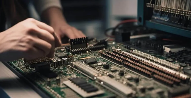
PCBA failure analysis helps teams understand why a circuit assembly stops working and how to improve production quality step by step. Modern electronic products use dense layouts and tiny packages, so even small process changes can influence performance. A clear analysis flow allows faster decisions and supports stable delivery schedules. Instead of guessing, teams rely on measurable inspection results and structured testing logic. As projects grow more complex, practical analysis methods become a daily requirement rather than a special task. This guide focuses on real workflows, useful tools, and prevention strategies that help improve consistency while keeping development efficient.

Why Do PCBA Failure Analysis?
Here are reasons why choose PCBA failure analysis:
- Improve product stability: Identify hidden defects early and increase assembly consistency across different production stages.
- Reduce repeated issues: Analysis helps locate the real source of abnormal behavior, allowing teams to refine design and process settings.
- Enhance production efficiency: Clear troubleshooting steps shorten investigation time and help maintain smooth delivery schedules.
- Support continuous improvement: Each analysis result provides data that can guide layout optimization, material selection, and assembly control.
- Strengthen quality control: Structured inspection methods help maintain stable standards and reduce variation between batches.
- Optimize cost management: Early detection minimizes rework, lowers scrap rates, and prevents large-scale production delays.
- Increase long-term reliability: Understanding failure patterns helps improve thermal design, solder joint performance, and environmental durability.
- Improve collaboration across teams: Clear analysis reports create a shared understanding between design, sourcing, and manufacturing groups.
What are the Most Common Causes of PCBA Failure?
Here are common causes of PCBA failure:
- Design-Related Causes
- Pad design mismatch: Pads that are too large or too small may lead to poor solder wetting or uneven joints.
- Component spacing too tight: Dense layouts increase the chance of solder bridging during reflow.
- Improper via placement: Unfilled via-in-pad structures can absorb solder and create weak connections.
- Thermal imbalance: Uneven copper distribution may cause parts to shift during heating.
- High-speed signal layout issues: Impedance errors can create unstable electrical behavior even when assembly looks correct.
- Soldering Process Causes
- Incorrect solder paste printing: Too much paste may create shorts, while insufficient paste can cause open joints.
- Unbalanced reflow profile: Rapid heating or cooling may stress components and lead to micro-cracks.
- Stencil design problems: Aperture size and thickness influence solder deposition accuracy.
- Flux residue: Remaining residue can attract moisture and affect long-term performance.
- Component Quality and Handling
- Oxidized component leads: Long storage periods may reduce solderability.
- Moisture-sensitive packages: Absorbed moisture can expand during reflow and damage internal structures.
- Incorrect orientation or placement: Slight misalignment may lead to uneven heating and weak solder joints.
- Mechanical stress during transport: Vibration can loosen small packages before testing begins.
- PCB Material and Surface Finish Factors
- Low Tg laminate in high-temperature applications: Material expansion may cause layer separation or solder fatigue.
- Surface finish compatibility: ENIG, OSP, or HASL finishes behave differently under repeated heating cycles.
- Copper thickness variation: Uneven copper distribution may create thermal imbalance during reflow.
- Contamination during fabrication: Residual chemicals can influence solder adhesion.
- Assembly Equipment and Process Control
- Placement accuracy tolerance: Worn feeders or calibration errors may shift component positions.
- Temperature uniformity inside reflow ovens: Uneven heating zones can produce inconsistent solder joints.
- Insufficient inspection checkpoints: Without SPI or AOI verification, small issues may pass unnoticed into later stages.
- Inconsistent cleaning processes: Residues left on the board may influence electrical behavior over time.
- Environmental and Operational Stress
- Thermal cycling: Repeated heating and cooling may weaken solder joints.
- Humidity exposure: Moisture can create leakage paths or corrosion.
- Electrostatic discharge: Static events may damage sensitive components without visible signs.
- Vibration and mechanical load: Automotive or industrial environments often introduce long-term stress.
- Human Factors and Workflow Gaps
- Incomplete documentation: Missing process notes may lead to repeated mistakes.
- Communication gaps between teams: Misunderstandings during design transfer can introduce hidden risks.
- Lack of standardized inspection criteria: Different teams may evaluate defects differently, causing inconsistent decisions
What are the Failure Modes of PCBA?
Failure modes of PCB assembly:
- Solder Joint Defects – Includes cold joints (insufficient heat during soldering), open joints (no electrical connection), and tombstoning (one end of a component lifts due to uneven soldering).
- Component Failure – Capacitors may dry out or short, resistors can crack/overheat, ICs may suffer from electrostatic discharge (ESD) or overvoltage damage.
- Thermal Issues – Overheating due to poor heat dissipation, causing solder joint reflow, component degradation, or PCB delamination.
- Mechanical Stress Damage – Vibration, bending, or impact can crack traces, break solder joints, or fracture components.
- Corrosion & Contamination – Moisture, flux residues, or environmental chemicals lead to electrochemical migration (ECM), short circuits, or corrosion.
- Electrical Overstress (EOS) – Excessive voltage/current damages components (e.g., gate oxide breakdown in MOSFETs).
- Design Flaws – Incorrect trace routing (impedance mismatch, signal integrity issues), inadequate grounding, or insufficient thermal relief.
- Manufacturing Defects – Poor solder paste application, misaligned components, or contamination during assembly.
- Counterfeit Components – Low-quality or fake parts fail prematurely due to substandard materials or processes.
- Aging & Wear – Repeated thermal cycling causes fatigue in solder joints and materials, leading to eventual failure.
What Tools Are Needed for Effective PCBA Failure Analysis?
Different tools reveal different layers of information. Combining several inspection methods produces a clearer picture.
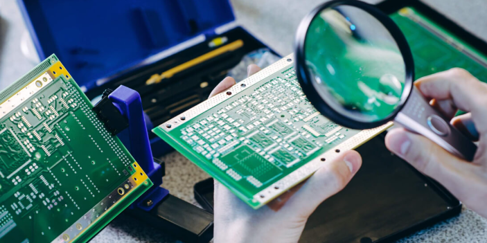
- Optical microscope: A microscope allows close observation of solder shape and alignment. Many visible defects become clear under magnification.
- X-ray inspection system: X-ray technology reveals hidden solder joints under packages like BGA or QFN. It helps detect voiding or insufficient solder.
- Digital multimeter: Voltage and resistance checks confirm whether signals flow correctly across the board.
- Oscilloscope: Signal waveform analysis shows timing problems or unstable power behavior.
- Thermal imaging camera: Heat patterns reveal uneven current flow or overloaded components.
- Cross-section equipment: Layer-by-layer inspection exposes plating quality and via structure when deeper investigation is required.
What Are Techniques of PCBA Failure Analysis?
Here are techniques for PCBA failure analysis:
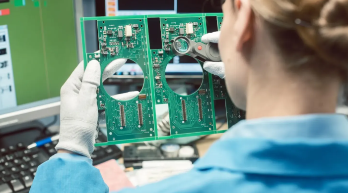
1. Visual Inspection (VI)
- Initial Screening: Manual/automated checks for solder bridges, missing components, pad damage, or tombstoning using magnifiers/AOI systems.
- Lighting Tricks: Angled lighting reveals micro-cracks; digital microscopes enable image comparison across batches.
- Surface Checks: Silkscreen clarity, pad oxidation, flux residue, or conformal coating integrity.
2. Automated Optical Inspection (AOI)
- Pattern Recognition: Compares solder volume/distribution across components; flags misaligned parts or polarity errors.
- Trend Analysis: Identifies recurring defects (e.g., pad lift) across production runs via image history tracking.
3. Electrical Testing
- Continuity/Shorts: Locates open circuits or unintended connections via bed-of-nails/flying probes.
- Dynamic Validation: Voltage probing during operation; signal integrity checks under load changes.
4. Functional Verification
- Real-World Simulation: Start-up timing, power-cycle stability, and load-dependent signal behavior testing.
- Reference Comparison: Cross-checks with known-good assemblies to isolate intermittent faults.
5. Thermal Analysis
- Infrared Imaging: Maps hotspots from high-resistance joints or overheating components; guides thermal design tweaks.
- Thermal Profiling: Compares temperature gradients to validate cooling strategies (e.g., heat sink placement).
6. X-Ray Inspection
- Subsurface Imaging: 2D/3D X-ray reveals hidden solder voids, BGA interconnections, or internal cracks.
- Void Analysis: Quantifies solder void percentages to assess joint reliability.
7. Cross-Section & Microstructure Analysis
- Destructive Sampling: Polished sections examine solder grain structure, via plating uniformity, or laminate delamination.
- Material Integrity: Checks intermetallic layer thickness and micro-crack propagation paths.
8. Surface/Material Analysis
- Contamination Detection: Ion chromatography identifies ionic residues (e.g., flux, salts) causing leakage currents.
- Elemental Verification: XRF confirms solder alloy composition (e.g., Pb-free compliance); SEM/EDS detects corrosion/tin whiskers.
9. Mechanical Stress Testing
- Flex/Vibration Tests: Simulates transport/installation stress; monitors solder joint stability under controlled flexing.
- Connector Durability: Repeated insertion cycles validate mechanical reliability.
10. Reliability Simulation
- Accelerated Aging: Thermal cycling, humidity exposure, and combined stress tests predict long-term performance.
- Environmental Chambers: Tests under controlled temperature/humidity to uncover latent defects.
11. Data Correlation & Process Review
- Root Cause Mapping: Links defects to process parameters (e.g., reflow profile, paste volume).
- Historical Analysis: Tracks recurring trends across production batches; documents lessons learned for future projects.
How to Perform a PCBA Failure Analysis?
Step-by-Step guide to PCBA failure analysis:
1. Initial Visual Inspection (Non-Destructive)
- Tools: Use a high-resolution stereo microscope (10-40x magnification) or digital microscope with adjustable lighting.
- Checklist:
- Solder joint quality: Look for cracks, voids, whiskers, or tombstoned components.
- Pad/trace integrity: Inspect for lifted pads, broken traces, or delamination.
- Component placement: Verify correct orientation (e.g., diodes, ICs), polarity (e.g., electrolytic caps), and alignment.
- Contamination: Identify flux residue, dust, or metallic debris using UV light if needed.
- Documentation: Capture high-resolution photos with scale markers for later comparison.
2. Electrical Testing (Functional Verification)
Continuity/Short Tests:
- Use a multimeter to check power rails (e.g., 3.3V, 5V) for shorts to ground or unexpected resistance.
- Employ automated test equipment (ATE) for boundary-scan or in-circuit tests (ICT) to validate component functionality.
Signal Integrity Checks:
- Use an oscilloscope to measure voltage levels, rise/fall times, and noise margins on critical signals (e.g., clocks, data lines).
- Perform parametric tests on passive components (e.g., capacitors for ESR, resistors for tolerance).
3. Advanced Imaging & Analysis
X-Ray Inspection:
- Utilize 2D/3D X-ray systems (e.g., Nordson YEST) to inspect hidden joints (e.g., BGAs, QFNs) for voids, head-in-pillow defects, or misalignment.
- Analyze X-ray images for solder distribution uniformity and component lead alignment.
Thermal Imaging:
- Use an IR camera (e.g., FLIR) to detect hotspots indicating high current paths, poor thermal management, or failing components.
4. Destructive Physical Analysis (DPA)
- Cross-Sectioning: Polish and etch solder joints to inspect intermetallic layers, voids, or cracks under a metallurgical microscope; Use SEM/EDS for high-magnification imaging and elemental analysis of fractures or contaminants.
- Component Decapsulation: Chemically etch IC packages to inspect die-level defects (e.g., bond wire lifts, die cracks) using SEM.
5. Environmental Stress Testing
Accelerated Life Tests:
- Subject the PCBA to thermal cycling (-40°C to +125°C), humidity (85% RH), or vibration (per MIL-STD-202) to replicate field failures.
- Monitor for intermittent faults using in-situ testing (e.g., continuous voltage monitoring during stress).
6. Root Cause Analysis & Reporting
- Data Synthesis: Cross-reference test results (visual, electrical, thermal) to identify patterns or correlations.
- Failure Mode Classification: Categorize defects (e.g., process-related, design-induced, component-specific).
- Corrective Actions: Recommend fixes (e.g., solder profile optimization, design rule changes, supplier audits) with risk assessments.
- Report Structure: Include executive summary, methodology, findings, root causes, and mitigation strategies with supporting images/data.
How to Efficiently Prevent PCBA Failures?
Below are methods to prevent PCBA failures:
- Design for Reliability (DFR) & Manufacturability (DFM): Optimize PCB layout with signal integrity analysis (e.g., impedance matching, crosstalk reduction) and thermal management (e.g., heat sinks, thermal vias). Use DFM rules to ensure solder pad geometries, component spacing, and trace widths meet manufacturing tolerances, preventing solder bridges or open circuits. For example, BGA pads should align with solder ball pitch to avoid voids.
- Component Selection & Supply Chain Control: Source high-quality components from certified suppliers with traceable batch records. Prioritize automotive-grade (AEC-Q200) or industrial-grade parts for harsh environments. Avoid counterfeit components through vendor audits and X-ray fluorescence (XRF) testing. Use Component Data Management (CDM) systems to track part parameters and lifecycles.
- Process Control & Cleanliness: Implement Statistical Process Control (SPC) for soldering parameters (temperature profiles, paste application). Maintain cleanliness with ultra-pure water rinsing and no-clean flux to prevent ionic contamination causing electromigration. Use automated optical inspection (AOI) and X-ray for void detection in solder joints. For example, J-STD-001 standards guide soldering processes.
- Environmental & ESD Protection: Control humidity (30–60% RH) and temperature (22–28°C) in production areas. Deploy ESD-safe workstations with wrist straps, ionizers, and conductive flooring. Use moisture barrier bags (MBBs) for component storage. For instance, ANSI/ESD S20.20 certifies ESD control programs.
- Testing & Validation: Perform In-Circuit Test (ICT) for component functionality, Functional Test (FCT) for end-use behavior, and Burn-In Test to screen early-life failures. Use HALT (Highly Accelerated Life Test) to identify design weaknesses. For example, IEC 61000-4 series tests EMC immunity.
- Documented Quality Systems: Adopt ISO 9001 or IATF 16949 for process documentation and continuous improvement. Maintain detailed production logs (e.g., solder paste stencil life, reflow oven calibration) for traceability. Use Failure Mode and Effects Analysis (FMEA) to proactively address risk areas like solder joint fatigue.
- Thermal & Mechanical Stress Mitigation: Design PCBs with thermal cycling in mind, use conformal coatings to protect against moisture and thermal shock. For high-vibration applications, reinforce connectors with epoxy or lock washers. For example, MIL-STD-883 tests mechanical shock resistance.
FAQs of PCBA Failure Analysis
Q1: What Is the First Step in PCBA Failure Analysis?
A1: The first step is to clearly define the symptom. Record when the issue occurs, under what conditions, and how it affects performance. Then perform a careful visual inspection using magnification. Many defects such as solder bridges, misalignment, or cracked joints can be identified early. Clear documentation at this stage saves time later.
Q2: How Do You Identify the Root Cause Instead of Just the Symptom?
A2: To find the root cause, move from surface observation to deeper verification. Compare the failed board with a known good sample. Perform electrical testing to confirm open or short circuits. Use X-ray or thermal imaging if needed. The goal is to identify the first event that triggered the abnormal behavior, not just the visible result.
Q3: When Should X-Ray Inspection Be Used?
A3: X-ray inspection should be used when defects are suspected under hidden packages such as BGA or QFN. It is helpful when visual inspection does not reveal clear issues. X-ray allows non-destructive evaluation of solder joints, voiding, and internal alignment. It is especially useful in high-density assemblies.
Q4: How Can Thermal Testing Support Failure Analysis?
A4: Thermal testing helps detect abnormal heat distribution. Infrared cameras reveal hot spots that may indicate excessive current or weak solder joints. Temperature cycling tests can also expose cracks caused by expansion stress. Thermal data often explains issues that only appear during operation.
Q5. How Can Failure Analysis Improve Future Production?
A5: Each analysis provides data that supports process refinement. Reviewing inspection results helps adjust solder paste volume, reflow profiles, or material selection. Over time, this reduces defect rates and improves assembly stability. Structured documentation ensures that lessons learned are applied to future builds.