 language
PCB Solder Mask: Material, Types & Process
The PCB solder mask is a crucial protective layer in printed circuit board (PCB) manufacturing, primarily used to prevent solder from adhering to non-soldering areas during soldering, thus avoiding short circuits, and protecting the copper traces from oxidation, mechanical damage, and environmental corrosion.
In this article, we will walk through PCB solder mask from an engineering and manufacturing perspective. We will focus on what it is, why it matters, how it is applied, and how to choose the right option for real production environments.
What Is PCB Solder Mask?
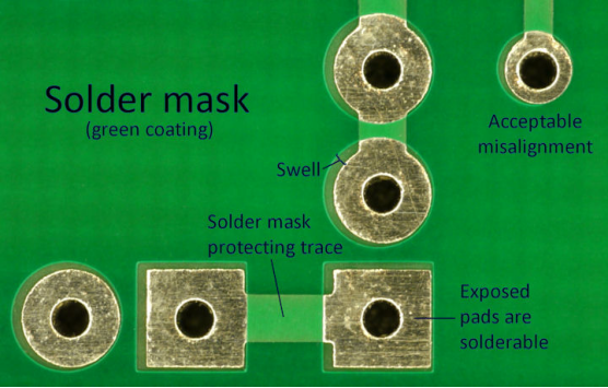
PCB solder mask is a thin protective coating applied to the surface of a printed circuit board. It covers copper traces while leaving pads, vias, and test points exposed for soldering and inspection.
In simple terms, it acts as a controlled barrier. It prevents solder from flowing where it should not. It also protects copper from oxidation, moisture, and minor mechanical damage.
From a manufacturing view, solder mask is not decoration. It is a functional layer that directly affects assembly quality. Without it, solder bridges become common, rework increases, and electrical reliability drops.
What is the Use of Solder Mask in PCB?
- Circuit Protection: Solder mask covers copper traces, preventing solder from adhering to non-soldering areas during soldering, avoiding short circuits.
- Insulation and Protection: Provides electrical insulation, protects circuits from oxidation, moisture, and mechanical damage, extending PCB lifespan.
- Soldering Assistance: Creates solder mask openings (exposing solder pads) to ensure accurate soldering areas, improving reliability and efficiency.
- Aesthetics and Identification: Typically green (or other colors) with silkscreen markings (e.g., component designators), enhancing readability.
What are the Different Types of Solder Masks?
Solder mask types are usually categorized by application method and curing mechanism:
- Liquid Photoimageable (LPI) Solder Mask: This is the most widely used option in modern PCB production. It is applied as a liquid, exposed through a photomask, and then developed. LPI solder mask offers high resolution and consistent thickness. It works well for fine-pitch designs and dense layouts.
- Dry Film Solder Mask: Dry film solder mask comes as a solid sheet that is laminated onto the board. It provides uniform thickness and sharp edges. However, it struggles with uneven surfaces and is less flexible for complex topography.
- Epoxy Solder Mask: Epoxy solder mask is applied by screen printing. It is durable and cost-effective for simple boards. That said, resolution is limited, making it less suitable for modern fine-line circuits.
What Color is the Standard PCB Solder Mask?
Below are colors of standard PCB solder mask:
- Green remains the most common PCB solder mask color. Green provides excellent contrast for copper and silkscreen. It also offers stable optical performance during inspection.
- Black gives a premium appearance but absorbs light, making inspection harder.
- Blue and red offer good balance between visibility and aesthetics.
- White is often used for LED boards but can discolor under heat.
- Yellow is sometimes chosen for high-contrast industrial designs.
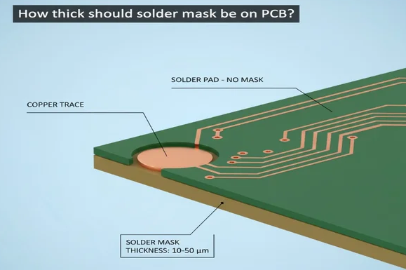
How Thick Should a Solder Mask be?
Most PCB solder mask layers have a thickness of 15–25 μm (0.015–0.025 mm), suitable for approximately 90% of typical applications. Special requirements include: high-frequency circuits require a reduced thickness of 10–15 μm to minimize the impact of the dielectric constant on the signal; high-power/enhanced insulation applications (such as power modules, industrial equipment) may require an increased thickness of 25–30 μm; special color inks (white, yellow, black) require a thickness of 25–35 μm due to coverage requirements.
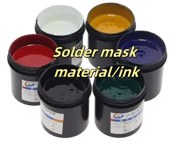
What Material is Used for Solder Masks for PCB?
- Most solder mask materials are epoxy-based polymers modified for heat resistance and chemical stability. These materials are designed to survive reflow temperatures and long-term environmental exposure.
- Modern PCB solder mask material formulations often include photo-initiators for UV exposure, pigments for color stability, and fillers for mechanical strength.
- High-reliability applications may require masks with enhanced thermal endurance, low ionic content, and strong adhesion to copper and laminate surfaces.
How to Apply Solder Mask on PCB?
Steps of PCB Solder Mask Process:
1. Pretreatment
- Surface cleaning: Alkaline degreaser ultrasonic cleaning for 5-10 minutes, oil residue ≤5mg/m²; micro-etching roughening uses ammonium persulfate solution to form Ra=0.3-0.5μm roughness, depth controlled at 1-1.5μm; 80℃ hot air drying for 5 minutes to prevent bubbles.
2. Solder Mask Ink Application
- Screen Printing: 600-mesh screen, squeegee pressure 0.2-0.3MPa, thickness deviation ≤±2μm, suitable for low-precision mass production boards.
- Spray Coating: Class 1000 cleanroom environment, nozzle distance 15-20cm from board, uniform coverage 15-25μm, ideal for complex structures.
- LPI Liquid Photoimageable: Precision 0.05mm, thickness 10-30μm controllable, mainstream for high-density boards, strong adhesion.
3. Pre-Baking
- Bake at 70-80℃ for 20-40 minutes, solvent residue ≤1%, hot air uniformity ≤±2℃ to prevent local overheating discoloration.
4. Exposure
- Conventional film exposure alignment tolerance ±0.05mm; LDI laser direct imaging offers higher precision, applicable to ≤0.1mm pitch BGA, UV triggers photopolymerization to cure solder mask areas.
5. Developing
- 1% sodium carbonate solution spray dissolves uncured ink, precise control of time and concentration to avoid under/over-developing.
6. Post-Curing
- Thermal curing: 140-150℃ baking for 30-60 minutes, epoxy resin fully crosslinked; UV-assisted curing enhances adhesion, hardness ≥6H pencil hardness.
7. Post-Processing
- Manual repair of pinholes/scratches; pad surface treatment (HASL/ENIG); reliability tests include hardness, solvent resistance (dichloromethane immersion verification).
How to Choose PCB Solder Mask Ink?
Choosing PCB solder mask ink should always start with the assembly process, not with color preference. Different inks respond differently to heat, chemicals, and surface finishes. A mismatch at this stage often shows up later as peeling, discoloration, or poor solder wetting.
First, consider reflow temperature. Lead-free assembly places higher thermal stress on the board. The solder mask ink must remain stable through multiple heat cycles without cracking or softening. For complex assemblies, thermal margin matters more than cost.
Next, evaluate electrical performance. High-voltage or fine-spacing designs benefit from inks with strong insulation resistance and low ionic contamination. This becomes especially important in humid or industrial environments where surface leakage can develop over time.
Then, look at compatibility with surface finishes. Some PCB solder mask inks bond better with ENIG, while others perform more consistently with HASL or OSP. Poor compatibility can lead to edge lifting around pads, which affects solder joint quality.
After that, factor in inspection and repair needs. Harder inks resist wear but are harder to remove during rework. Softer inks simplify touch-up but may scratch more easily. The right balance depends on product lifecycle and service expectations.
Finally, think about long-term appearance. Color stability, gloss level, and resistance to yellowing all influence how the board looks after aging and thermal exposure. For consumer or visible products, this detail carries real value.
How to Remove Solder Mask from PCB?
Comprehensive Analysis of PCB Solder Mask Removal Methods
- Physical Scraping/Polishing Method
- Applicable Scenario: Small-area repairs (<5mm²) or scenarios without professional equipment
- Tools: Surgical blade/precision scraper (blade angle ≤15°), fiberglass pen (0.5-1mm tip)
- Operation: Secure PCB on anti-slip pad, scrape at 10-20° angle with light repeated strokes until copper surface is bright; fiberglass pen suitable for BGA adjacent micro-areas
- Risk: Must wear N95 mask + goggles + dust extraction device; avoid unidirectional force to prevent fiberglass tearing
- Chemical Solvent Softening Method
- Applicable Scenario: Thermally cured solder mask or local large-area removal (UV-cured solder mask may be ineffective)
- Solvent Selection: Dichloromethane-based paint remover (high efficiency, high toxicity), acetone (only for incomplete curing), specialized stripping agents
- Process: Operate in explosion-proof fume hood; apply solvent with cotton swab ≤3 minutes, remove softened material with polyimide scraper, rinse with IPA followed by 60°C drying for 5 minutes
- Safety: Requires nitrile gloves + chemical mask; perform compatibility testing on board edge non-circuit areas first
- Laser Ablation Method
- Applicable Scenario: HDI board fine-tuning/batch processing (accuracy ±10μm)
- Technical Parameters: UV laser (355nm, energy 3-5J/cm²) suitable for LPI solder mask; CO₂ laser (10.6μm) requires heat-affected zone control
- Advantages: Non-contact, chemical-free pollution, supports CAD file precise positioning, ideal for RF circuit impedance matching zone correction
- Design Software Correction Method
- Preventive Strategy: Set pad property Solder Mask Expansion=Tented in EDA software; negative values (-50% pad size) can completely eliminate openings
- Verification: Enable DRC to check solder mask bridge width (≥4mil) and opening boundaries; prioritize design optimization to minimize rework (especially in BGA/0201 component areas)
- Method Selection Decision Table
| Method | Accuracy (μm) | Applicable Area | Risk Level | Cost |
| Physical Scraping | ±50 | <5cm? | High | Low ($<10) |
| Chemical Dissolution | ±100 | <20cm? | Extremely High | Medium ($20-50) |
| Laser Ablation | ±10 | Any | Low | High (>$5k) |
| Design Optimization | Software-defined | Full board | Zero | Engineering time only |
Safety and Reliability Guidelines
- Physical/Chemical Methods: Strictly prohibit scraping gold/ENIG pads; post-treatment requires IPC-570 ionic contamination testing
- Laser Method: Control pulse frequency on FR4 substrate to prevent carbonization; post-repair requires electron microscopy for copper surface scratch inspection and impedance testing
FAQs of Circuit Board Solder Mask
Q1: Is solder mask necessarily green?
A1: No, green is the standard color, but it can be produced in various colors according to requirements.
Q2: Does solder mask thickness affect soldering?
A2: Yes, both excessive thickness and insufficient thickness can lead to poor soldering, such as solder bridges or cold joints.
Q3: What is the difference between solder mask and paste mask?
A3: Solder mask is the solder resist layer that defines areas not to be covered by green oil (i.e., pads), while paste mask (stencil) is a template that defines the location for solder paste deposition.
Q4: How much larger should the solder mask opening be compared to the pad?
A4: It is generally recommended that the solder mask opening should be 0.1mm to 0.2mm (0.004 inches to 0.008 inches) larger than the pad to ensure soldering reliability.
Q5: How to check the quality of solder mask?
A5: Inspect visually for defects such as bubbles, cracks, and poor adhesion, and use a microscope to check the opening dimensions and edge neatness.