 language
What File Type Is Used for PCB Schematic Drawings? (Complete Guide 2025)
Designing a printed circuit board (PCB) begins long before traces and copper layers are drawn. The first and most important step in any electronic design is creating the schematic drawing — a graphical representation of how electronic components are connected and how signals flow within a circuit.
This schematic is the blueprint for the PCB layout, manufacturing, and assembly processes. Understanding its file types, structure, and role in the design workflow is essential for engineers, technicians, and electronics manufacturers.
What Format Is a PCB Schematic File?
PCB schematic drawings are created and stored using Electronic Design Automation (EDA) software tools. Each EDA platform uses its own file format and extension, which contains information about circuit components, symbols, connections (nets), and attributes like pin names or reference designators.
Below is an overview of the most commonly used schematic file types in the electronics industry:
| Software | Schematic File Extension | Description |
| Altium Designer | .SchDoc | Professional-grade schematic file supporting complex hierarchical designs. |
| Autodesk EAGLE | .sch | Common for smaller projects and hobbyist-level designs. |
| KiCad | .sch (up to v5), .kicad_sch (v6+) | Open-source schematic format with strong community support. |
| OrCAD Capture | .dsn | Widely used in commercial and industrial PCB design. |
| PADS Logic (Mentor Graphics) | .sch | Preferred by enterprise engineers for robust design workflows. |
| Proteus | .dsn | Combines schematic capture with simulation tools. |
| EasyEDA | Cloud-based JSON structure | Web-friendly format allowing easy sharing and collaboration. |
For documentation or communication, engineers often export schematics into PDF, SVG, or DXF. These are non-editable but easy to read. The original file, however, must remain in its native format, as it contains all the electrical rules, netlists, and metadata needed for simulation and PCB layout.
Why PCB Schematic Drawings Are Important in PCB Design?
A schematic drawing defines electrical relationships between all components in a circuit. It captures logical connections—how resistors link to capacitors, how IC pins are tied to sensors, and how signals flow through circuits. Engineers use it to verify circuit theory before any copper is etched or any board is assembled.
Here’s why schematic drawings are essential in PCB design:
1. Electrical Verification: Schematic data drives Electrical Rule Checks (ERC) to catch short circuits or open nets early.
2. Bill of Materials (BOM) Creation: The schematic links each part with its electrical parameters and manufacturer details.
3. Design Communication: It bridges communication between design, layout, and manufacturing teams.
4. Signal Integrity Control: Engineers can analyze critical nets, impedance paths, and grounding schemes directly from schematic connectivity.
5. Error Prevention: Mistakes at the schematic stage are easier and cheaper to correct than at fabrication.
A well-designed schematic guarantees that the physical PCB performs exactly as the designer intended. It’s the “language” that every team—engineering, manufacturing, and testing—can understand.
Common Component Symbols Used in PCB Schematic Drawings
Schematic diagrams use standardized symbols to represent real-world components. Each symbol tells a story: how the part behaves, its function, and its connections. Recognizing these symbols is key to understanding the entire design.
Here are the most common symbols you’ll encounter:
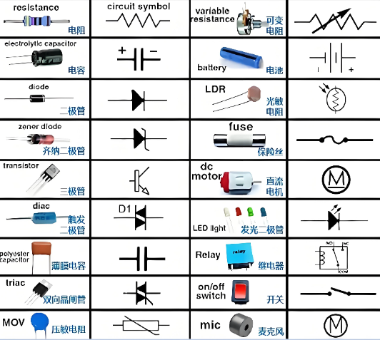
Each component connects through nets, which are the electrical “wires” in schematic form. Dots mark junctions, and net labels indicate signal names like “CLK,” “TX,” or “GND.”
Symbols may vary slightly between EDA tools, but their meaning remains consistent. Once you can interpret these, you can read almost any schematic worldwide.
How to Read a PCB Schematic Drawing?
Reading a schematic is a fundamental skill for engineers, technicians, and students. A schematic is essentially a map of electrical pathways, and learning to interpret it involves recognizing symbols, tracing signal paths, and understanding design intent.
Steps to Read a PCB Schematic:
- Start with Power and Ground Lines: Identify where power enters (VCC, VDD) and where ground (GND) connects. This forms the reference framework of the circuit.
- Follow the Signal Flow: Most schematics are organized logically from left (input) to right (output). Trace how the signal moves between components.
- Recognize Component References: Each component is labeled (e.g., R1, C2, U5), corresponding to actual components on the PCB layout.
- Understand Nets and Labels: Nets define how pins are connected. Long or complex connections often use net labels rather than drawn wires for clarity.
- Check Junctions and Crossings: A dot at the intersection of lines means a connection; lines that cross without dots typically do not connect.
- Review Multi-Sheet Schematics: For large circuits, multiple schematic pages are linked by off-page connectors or hierarchical labels.
Reading schematics becomes more intuitive with practice, especially once you become familiar with symbol conventions and design patterns.
How to Convert PCB to Schematic Diagram?
In some cases, a finished PCB exists without its original schematic file. This is common when dealing with legacy hardware, competitor analysis, or replicating discontinued electronics. The process of extracting a schematic from a physical PCB is known as PCB reverse engineering.
The Process of PCB-to-Schematic Conversion
- Capture PCB Images: Scan or photograph both sides of the board in high resolution.
- Identify Components: Label all visible components, noting part numbers and pin orientation.
- Trace Copper Paths: Use optical or digital tracing to map the electrical connections between components.
- Generate a Netlist: Software tools can analyze the connections to create a digital netlist (a list of all electrical connections).
- Reconstruct the Schematic: Import the netlist into an EDA tool (such as Altium, KiCad, or OrCAD) to recreate the schematic diagram.
- Verify Manually: Compare the recreated schematic to the physical PCB to ensure accuracy.
Common Reverse Engineering Tools
- ScanCAD Systems
- REVERSE CAD
- Altium Reverse Engineering Toolkit
- Zuken CR-5000 or PADS Reverse Tools
While reverse engineering can automate netlist extraction, manual validation is always required to guarantee the resulting schematic’s correctness.

Software Used for Electronic Schematic Drawing
A wide range of software tools are available for schematic design, each offering different capabilities for component libraries, simulation, and PCB integration.
| Software | Type | Highlights |
| Altium Designer | Professional | Industry-leading software for advanced PCB and schematic design, with powerful simulation and collaboration tools. |
| KiCad | Free / Open Source | Full-featured EDA suite with strong community support and no licensing fees. |
| Autodesk EAGLE | Commercial / Free for hobby use | Intuitive tool popular among makers and startups. |
| OrCAD Capture (Cadence) | Professional | Trusted in enterprise-level and high-reliability industries. |
| Proteus Design Suite | Commercial | Combines schematic capture with microcontroller simulation. |
| EasyEDA | Free / Cloud-based | Web-based schematic editor integrated with PCB manufacturing (JLCPCB). |
| NI Multisim | Commercial | Excellent for education and analog circuit simulation. |
| DipTrace | Paid / Trial | User-friendly schematic and PCB design tool with a short learning curve. |
Each EDA tool uses its own file format — such as .SchDoc, .sch, or .dsn — but all serve the same purpose: to accurately describe the electrical logic of a circuit. Whether you are designing new products, analyzing legacy boards, or learning electronics, understanding schematic drawings is essential to mastering PCB design.
Frequently Asked Questions (FAQs)
1. What is the difference between a schematic and a PCB layout?
A schematic is a logical diagram showing electrical connections between components, while a PCB layout is the physical arrangement of components and traces on the circuit board.
2. Can I open a schematic file from one software in another?
Usually not directly. Each EDA tool uses a proprietary format, but you can export and import using netlists, EDIF, or PDF for cross-compatibility.
3. How can I print or share a schematic drawing?
Most EDA software allows exporting to PDF, SVG, or PNG for easy sharing and documentation.
4. What is a netlist, and how is it related to a schematic?
A netlist is a text-based representation of all electrical connections (nets) in a circuit. It’s generated from a schematic and used during PCB layout and manufacturing.
5. Can a schematic file be simulated?
Yes. Many schematic editors include built-in or third-party simulation engines (SPICE-based) to analyze circuit behavior before physical prototyping.
6. Is it legal to reverse engineer a schematic from a PCB?
Reverse engineering is generally legal for maintenance, education, or interoperability, but duplicating or selling someone else’s copyrighted design is prohibited.