 language
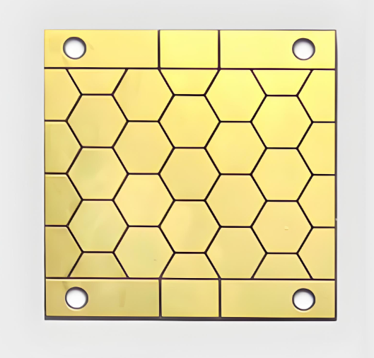
What Is DCB Ceramic PCB? DBC Ceramic PCB
A DCB (Direct Copper Bonded) Ceramic PCB, also known as DBC (Direct Bonded Copper), is a high-performance substrate where copper foil is directly bonded to a ceramic base—commonly Al₂O₃ (Alumina) or AlN (Aluminum Nitride)—under high temperature. This advanced process produces a structure that merges superior thermal performance with excellent electrical insulation.
Unlike traditional FR4 boards, DCB ceramic PCBs can handle higher currents, dissipate more heat, and maintain stable performance under extreme temperature conditions. Their unique construction makes them the go-to choice for power electronics, automotive control units, and high-power semiconductor devices.
How Does DBC Ceramic Technology Work?
DCB technology involves bonding thick copper layers (typically 0.1–0.3mm) directly onto the ceramic substrate using a copper-oxygen eutectic reaction at temperatures around 1065°C. The reaction forms a thin Cu–O–Al interface layer, ensuring strong metallurgical adhesion without any intermediate adhesive materials.
This process provides low thermal resistance, high insulation strength, and mechanical durability—ideal for high-current, high-temperature operations.
Key Characteristics of DBC Ceramic PCB
- High Mechanical Strength: Exceptional durability and shape stability under stress.
- Superior Thermal Conductivity: Efficient heat dissipation for high-power applications.
- Excellent Electrical Isolation: Prevents breakdowns and improves circuit safety.
- Outstanding Thermal Cycling Capability: Can withstand over 50,000 thermal cycles.
- Fine Solderability and Corrosion Resistance: Maintains performance in harsh environments.
- Wide Operating Temperature: Reliable performance from -55°C to 850°C.
- Eco-Friendly: Free from toxic materials like BeO, safe for the environment.
These features make DCB ceramic PCBs suitable for COB (Chip on Board) packaging and power modules, representing the future trend of compact, reliable, and energy-efficient electronics.
DBC Ceramic PCB vs. Thin Film & Thick Film Ceramic PCB
| Feature | DCB Ceramic PCB | Thick Film Ceramic PCB | Thin Film Ceramic PCB |
| Conductor Thickness | 0.1–0.3mm | 10–13µm | <10µm |
| Thermal Conductivity | Very High | Moderate | Moderate |
| Current Capacity | Very High | Medium | Low |
| Production Cost | Higher | Lower | Medium |
| Etching Capability | Excellent | Good | Good |
| Typical Use | Power modules, automotive electronics | Sensors, control boards | Precision circuits |
DCB ceramic PCBs stand out due to their exceptional current handling and thermal stability, making them ideal for power electronics and energy systems.
Advantages of DBC Ceramic PCB
- Low Thermal Resistance: The direct bonding process minimizes heat transfer barriers, enhancing efficiency.
- High Current Carrying Capacity: Supports up to 100A current with minimal temperature rise.
- Closer Thermal Expansion to Silicon: Reduces mechanical stress during operation, ideal for chip soldering.
- Reduced Solder Layer: Fewer interfaces mean lower costs and improved reliability.
- Enhanced System Reliability: Compact packaging increases power density while maintaining safety.
- Non-Toxic Replacement for BeO: Eliminates environmental and health concerns associated with beryllium oxide.
- Improved Insulation Voltage: Offers better personnel and equipment protection.
- Customizable Layout: Can be etched like normal FR4 PCB, supporting versatile circuit designs.
Example:
A 0.3mm copper layer on a DCB board with a 1mm trace width carries 100A current continuously, with only a 17°C temperature rise, and just 5°C rise with a 2mm trace width.
Thermal Performance of DBC Ceramic Substrate
| Substrate Thickness | Thermal Resistance (K/W) | Heat Dissipation |
| 0.25mm | 0.14 | Excellent |
| 0.38mm | 0.19 | Very Good |
| 0.63mm | 0.31 | Good |
Lower thermal resistance means more effective heat transfer, leading to longer component life and enhanced system efficiency.
Applications of DBC Ceramic PCB
- Automotive Electronics: Inverters, battery management systems (BMS), and motor controllers.
- Power Modules: IGBTs, MOSFETs, and high-current rectifiers.
- LED Lighting: High-brightness LEDs requiring efficient thermal dissipation.
- Aerospace and Defense: High-reliability power and RF modules.
- Renewable Energy: Solar inverters and wind turbine controllers.
- Industrial Automation: Servo drives and robotics power systems.
Why Choose Best Technology for DCB Ceramic PCBs?
Best Technology is a trusted DCB ceramic PCB manufacturer offering customized DCB solutions for high-power applications.
We specialize in AlN and Al₂O₃ DCB substrates, with precise copper thickness control, fine etching, and strict thermal cycle testing.
Our Advantages
- 19 years ceramic PCB manufacturing experience
- Advanced bonding and etching processes.
- High-purity ceramic materials for consistent insulation.
- Various raw material options: Al2O3, BeO, Si3N4,
- Tight tolerance control for copper thickness.
- Certifications: ISO9001, ISO13485, IATF16949, and AS9100D.
- Competitive pricing and professional engineering support.
If you need reliable high-power ceramic PCBs, Best Technology is your one-stop solution.
DBC Ceramic PCB Manufacturing Capability from Best Technology
Best Technology has fabricated and supplied DBC ceramic board for many years, our full set of high-tech machines and a series of test equipment such for AOI, resistance measurement, two-dimensional testers support us to make high quality and defective-free products for our customers. Below are the manufacturing capabilities for DBC ceramic PCB:
| Item | DCB/DBC Capabilities |
| Layer Count | 2 Layers |
| Max Board Dimension | 138*178mm |
| Min Board Thickness | 0.30mm.0.40mm |
| Max Board Thickness | 1L: 1.3mm; 2L 1.6mm |
| Conductor Thickness | 3.90Z-8.60z |
| Min Line Width/Line Space | 12/12mil (0.30/0.30mm) |
| Substrate Type | AI203,ALN, Zro2 |
| Substrate Thickness | 0.25, 0.38, 0.50, 0.635, 0.76,1.0mm |
| Min Hole Diameter | 4mil (0.1mm) |
| Min Hole Spacing | NPTH: 16mil (0.30mm); PTH: 20mil (0.5mm) |
| Min PAD Ring(Single) | N/A |
| PTH Wall Thickness | N/A |
| Min Solder PAD Dia | 8mil (0.20mm) |
| Min Soldermask Bridge | 8mil(0.20mm) |
| Min BAG PAD Margin | 8mil (0.20mm) |
| PTH/NPTH Dia Tolerance | PTH: ±4mil (0.1mm) ; NPTH: ±2mil (0.05mm) |
| Hole Position Deviation | ± 4mil (0.1mm) |
| Outline Tolerance | Laser: +0.2/0.05mm |
| Line Width/Spac Tolerance | +5mil (0.125mm) |
| Surface Treatment | OSP/Ni Plating, ENIG |
| Thermal Stress | 3 x 10 Sec @ 280C |
FAQs About DCB Ceramic PCB
Q1: What materials are commonly used in DCB ceramic PCBs?
A1: The most common base materials are Al₂O₃ (Alumina) and AlN (Aluminum Nitride), each offering different levels of thermal conductivity and mechanical strength.
Q2: What is the maximum copper thickness for DCB PCBs?
A2: Typically, the copper thickness ranges from 0.1mm to 0.3mm, depending on current requirements and design.
Q3: Can DCB ceramic PCBs replace BeO substrates?
A3: Yes, they provide similar thermal performance without the toxicity issues of BeO, making them a safer and more sustainable option.
Q4: What is the main application of DCB substrates?
A4: DCB substrates are mainly used in power semiconductor modules, automotive electronics, LEDs, and renewable energy systems.
Q5: Why is DCB preferred for high-power circuits?
A5: Because of its low thermal resistance, high mechanical stability, and direct copper bonding, which supports efficient heat dissipation and high reliability.