PCB Design

PCB Design

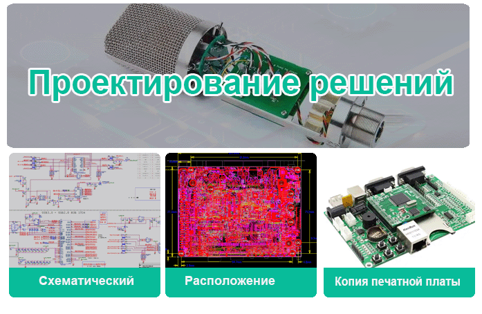
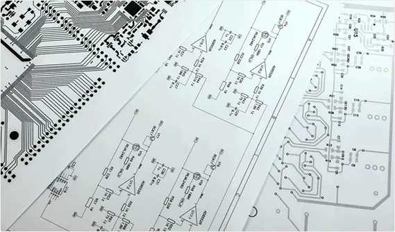
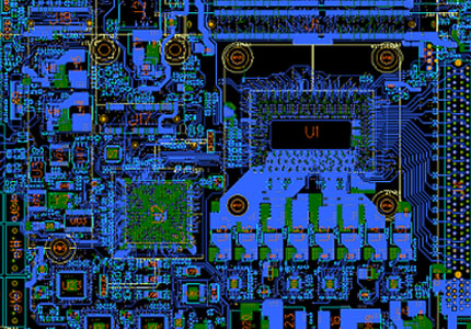
Printed circuit board (PCB) design is based on circuit schematics to realize the functions required by the circuit designer. This is a complex process that includes several steps, such as schematic drawing, layout design, DFM and testing.

A good PCB design can create functional, reliable, and cost-effective circuit boards that meet the electrical and physical requirements of the devices they will be used in. PCB design is critical to ensuring the proper operation of devices and minimizing the risks of electrical shorts, interference, and other problems that can arise from poor design. PCBs are widely used in various electronic devices, from small consumer products to large industrial machines.

PI Analysis
PI Analysis

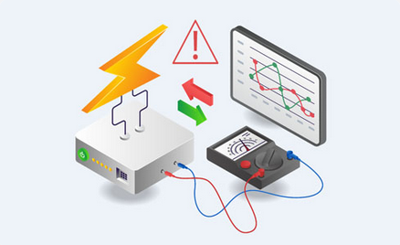
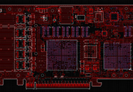
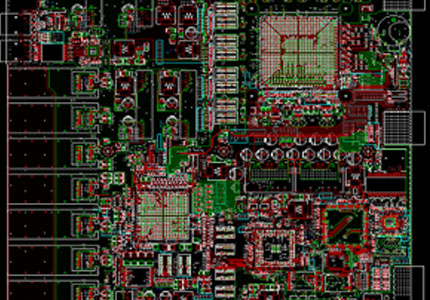
Power Integrity (PI) Analysis focuses on managing the power distribution network to minimize noise, voltage drops, and other power-related issues. It involves evaluating the power distribution network within a PCB to ensure all components receive stable and adequate power.

Get instant quote
SI Analysis
SI Analysis

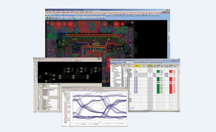
Signal Integrity (SI) Analysis can assess and optimize the quality of electrical signals as they travel through a PCB. It is mainly used to maintain the integrity of signals, especially in high-speed circuits, so that they can transmit without distortion or degradation. SI analysis solves issues such as signal reflection, crosstalk, and electromagnetic interference.

Get instant quote
EMC Test
EMC Test

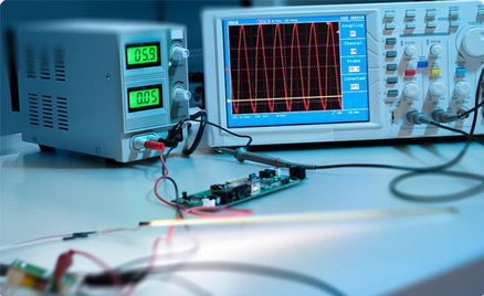
For every new PCB case, electromagnetic compatibility (EMC) is an important process in the development and certification of electronic devices. By evaluating a device's ability to function properly in its intended electromagnetic environment while limiting the unintentional generation, propagation, and reception of electromagnetic energy, we can make sure the device does not cause interference with other electronic equipment and can withstand external electromagnetic disturbances.

Get instant quote
PCB Design Process

PCB Design Process

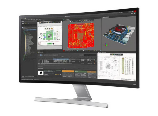
We uphold the following design principle: cost-effectiveness, security, compliance, performance, reliability and time to market.

Throughout the design process, we’ll collaborate with you on any required design changes and provide suggestions to improve your new product.

  • Schematic Capture
  • PCB Stackup Design
  • PCB Layout and Routing
  • Verification in Simulations
  • PCB Design Review
  • PCB Manufacturing File Creation
Get a free consultation

PCB Design Cases

Full turnkey PCB design served for more than 1700 customers, include but are not limited to BYD, DIDI, HUAWEI.

1Industrial Motherboard Design

Industrial Motherboard Design

  • Intel Xeon E3, Core™ i7
  • 2x DDR4 SODIMM 2133 MHz
  • 4x SATA Gen 3.0
  • 1x PCIe x16 (Gen 3)
  • 2x USB 3.0 (Internal)
2PCB Design for PCIe Card

PCB Design for PCIe Card

  • Main chip: XCKU11P
  • 30A maximum current
  • Single pair differential line, 10G optical network
  • 14 layers PCB
3Network Motherboard Design

Network Motherboard Design

  • BCM88XXX, BCM55XXX chips
  • 60A maximum current
  • 8X10G optical network
  • 8 x DDR3 chips

ABOUT US

Founded on June 28, 2006, Best Technology is committed to providing one-stop PCB solutions to drive technological advancement and innovation. With over 19 years of experience, we have become a trusted partner for clients worldwide, offering best solutions to meet the growing needs of the electronics industry.

pcb in Vietnam

Company Profile

Our products range from standard FR4 PCB, multi-layer PCBs, metal-based PCBs (MCPCBs), ceramic PCBs, flexible and rigid-flexible PCBs to high frequency PCBs. Currently our monthly capability is 260,000 square feet (28,900 square meter), more than 1,000 different boards will be completed. We also provide expedite service, so that urgent boards can be shipped out within 24 hours.

As a custom printed circuit board manufacturer, we believe that continuous growth is the key to success. So, we always invest heavily in research and development to stay ahead of industry trends. We focus on product quality and customer satisfaction, and we aim to build strong relationships and offer personalized support and solutions to our customers.

pcb manufacturer in Vietnam

Quality certification

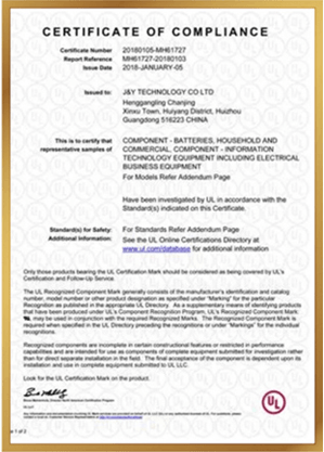
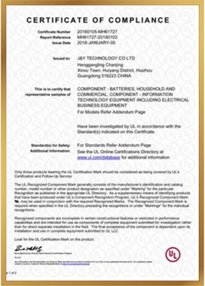
Are you worried about quality certification? Don't worry, we have the relevant quality certifications and a RoHS-compliant quality management system to ensure good PCB quality.

  • IATF 16949
  • ISO 9001:2015
  • ISO 13485:2016
  • AS9100D
  • REACH
  • RoHS
  • UL

WHY CHOOSE US?

With 18 years of experience in PCB manufacturing and assembly, we offer competitive factory prices and short lead times to ensure your schedule runs smoothly.

01 Competitive prices

Competitive prices

We are committed to providing high-quality PCB solutions at competitive prices. By optimizing manufacturing processes and managing costs effectively, we ensure you receive the best value for your investment.

01 02Quality assurance

Quality assurance

At Best Technology, quality is our top priority. We implement rigorous quality control processes throughout every stage of production, from raw material selection and prototyping to final product testing.

01 03 All-inclusive service

All-inclusive service

Our all-in-one approach simplifies the supply chain, shortens lead times, and improves communication efficiency. And we offer one-on-one sales assistant services to give you a superior experience working with us.

01 04 On-time

On-time delivery

We understand the importance of meeting your project deadlines, and we provide online WIP updates to ensure you can track the progress of your PCB product.

Frequently Asked Questions

Why is my 4-layer PCB experiencing signal interference, and how do I fix it?
Signal interference often stems from incorrect layer stack order—ensure signal layers (Top/Bottom) are adjacent to reference planes (GND/Power). Avoid placing power and ground planes in reverse order, and use continuous reference planes for high-speed signals to minimize reflection. Use the Layer Stack Manager in your design tool to reorder layers, and run a signal integrity analysis before finalizing.
How do I resolve impedance control mismatches in Altium Designer?
Mismatches happen when layer spacing, copper thickness, or material parameters are off. Enable the Impedance Calculation feature in Layer Stack Manager, input your substrate’s dielectric constant (FR4 = 4.4 typical), and adjust layer spacing (0.2–0.4mm for signal-GND layers). Double-check that your trace width matches the calculated impedance (50Ω or 100Ω for differential pairs).
My PCB design fails DRC checks due to power plane splitting—what’s wrong?
Power plane splitting errors usually come from insufficient spacing between voltage domains (e.g., 3.3V and 5V) or crossed signal paths. Use the Split Planes tool to create clear boundaries between power regions, leave at least 1mm spacing between splits, and avoid routing signals across different power domains. Run a DRC check after splitting to catch overlaps.
Why won’t my PCB’s inner power layer connect properly to components?
This is often caused by not enabling the Negative Layer option for inner power/GND layers. In your design tool, go to layer properties and select "Negative Layer" for inner planes. Use Plane Connect (not Net Tie) to link components to the power layer, and ensure vias are set to "Thermal Relief" to prevent cold joints during manufacturing.
As a beginner, which PCB design software should I choose—KiCad, Altium, or Eagle?
KiCad is best for hobbyists/beginners (free, open-source, strong community support). Altium Designer works for professionals (robust for high-speed, multi-layer designs but paid). Eagle balances ease of use and features (good for small-to-medium projects). Start with KiCad to learn basics, then switch to Altium if you need advanced tools for industrial projects.
How do I choose the right substrate material for my PCB design?
FR4 is the standard for most consumer electronics (affordable, good electrical performance). Use high-frequency substrates (e.g., Rogers) for RF/microwave designs, and flexible substrates (e.g., polyimide) for wearable devices. Consider operating temperature—industrial PCBs may need heat-resistant materials to avoid warping.
What’s the biggest mistake new PCB designers make, and how to avoid it?
Skipping design rule checks (DRC) and ignoring manufacturability. Always run DRC before sending files to manufacturing—pay attention to minimum line spacing, hole sizes, and trace width. Consult your manufacturer’s design guidelines (e.g., minimum feature sizes) early in the process to avoid rework.
How can I reduce EMI in my PCB design without increasing costs?
Keep power loops small by placing decoupling capacitors close to IC power pins. Use solid ground planes instead of ground traces, and avoid long, parallel signal traces (they cause crosstalk). Ensure power and ground planes are properly paired, and route high-speed signals (e.g., USB, HDMI) away from power traces.
Why do my PCB prototypes have soldering issues, and how to fix it?
Soldering problems often relate to pad size or thermal relief settings. Make sure pad sizes match component leads (follow IPC standards), and use thermal relief vias for large pads (prevents heat dissipation during soldering). Avoid placing components too close together—leave at least 0.5mm spacing for assembly access.
How do I verify my PCB design is ready for manufacturing?
Run a full DRC check (fix all errors, not just warnings). Generate and review Gerber files (ensure all layers are included: signal, power, silkscreen, solder mask). Use a 3D viewer to check component placement and mechanical fit. Send a sample design to your manufacturer for a pre-production review—most offer free checks for manufacturability.

years of dedicating to PCB Assembly

Simply drop your email or phone number in the contact form, and we'll promptly provide you with a quotation.